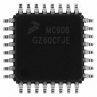
MC908GZ60CFJE Freescale Semiconductor, MC908GZ60CFJE Datasheet - Page 178

MC908GZ60CFJE
Manufacturer Part Number
MC908GZ60CFJE
Description
IC MCU 60K FLASH 8MHZ 32-LQFP
Manufacturer
Freescale Semiconductor
Series
HC08r
Datasheet
1.MC908GZ60CFJE.pdf
(352 pages)
Specifications of MC908GZ60CFJE
Core Processor
HC08
Core Size
8-Bit
Speed
8MHz
Connectivity
CAN, SCI, SPI
Peripherals
LVD, POR, PWM
Number Of I /o
21
Program Memory Size
60KB (60K x 8)
Program Memory Type
FLASH
Ram Size
2K x 8
Voltage - Supply (vcc/vdd)
3 V ~ 5.5 V
Data Converters
A/D 24x10b
Oscillator Type
Internal
Operating Temperature
-40°C ~ 85°C
Package / Case
32-LQFP
Controller Family/series
HC08
No. Of I/o's
21
Ram Memory Size
2KB
Cpu Speed
8MHz
No. Of Timers
2
Embedded Interface Type
CAN, SCI, SPI
Rohs Compliant
Yes
Processor Series
HC08GZ
Core
HC08
Data Bus Width
8 bit
Data Ram Size
2 KB
Interface Type
CAN, ESCI, SPI
Maximum Clock Frequency
8 MHz
Number Of Programmable I/os
53
Number Of Timers
8
Maximum Operating Temperature
+ 85 C
Mounting Style
SMD/SMT
Development Tools By Supplier
FSICEBASE, DEMO908GZ60E, M68EML08GZE
Minimum Operating Temperature
- 40 C
On-chip Adc
10 bit, 24 Channel
Lead Free Status / RoHS Status
Lead free / RoHS Compliant
Eeprom Size
-
Lead Free Status / Rohs Status
Details
Available stocks
Company
Part Number
Manufacturer
Quantity
Price
Company:
Part Number:
MC908GZ60CFJE
Manufacturer:
Freescale
Quantity:
4 000
Company:
Part Number:
MC908GZ60CFJE
Manufacturer:
Freescale Semiconductor
Quantity:
10 000
- Current page: 178 of 352
- Download datasheet (5Mb)
Input/Output (I/O) Ports
13.5 Port C
Port C is a 7-bit, general-purpose bidirectional I/O port. Port C also has software configurable pullup
devices if configured as an input port. PTC[1:0] are shared with the MSCAN module.
13.5.1 Port C Data Register
The port C data register (PTC) contains a data latch for each of the seven port C pins.
PTC6–PTC0 — Port C Data Bits
CAN
13.5.2 Data Direction Register C
Data direction register C (DDRC) determines whether each port C pin is an input or an output. Writing a 1
to a DDRC bit enables the output buffer for the corresponding port C pin; a 0 disables the output buffer.
178
These read/write bits are software-programmable. Data direction of each port C pin is under the control
of the corresponding bit in data direction register C. Reset has no effect on port C data.
The CAN
MSCAN08 control register determines, whether the PTC1/CAN
pins or general-purpose I/O pins. See
RX
and CAN
Alternate Function:
RX
Address:
–CAN
Bit 6 through bit 2 of PTC are not available in the 32-pin LQFP package.
Reset:
Read:
Write:
Address:
TX
Reset:
Read:
Write:
MC68HC908GZ60 • MC68HC908GZ48 • MC68HC908GZ32 Data Sheet, Rev. 6
— MSCAN08 Bits
TX
$0006
pins are the MSCAN08 modules receive and transmit pins. The CANEN bit in the
Bit 7
0
0
$0002
Bit 7
Figure 13-10. Data Direction Register C (DDRC)
1
= Unimplemented
Figure 13-9. Port C Data Register (PTC)
DDRC6
= Unimplemented
6
0
PTC6
6
DDRC5
Chapter 12 MSCAN08 Controller (MSCAN08).
5
0
PTC5
5
NOTE
DDRC4
4
0
Unaffected by reset
PTC4
4
DDRC3
3
0
PTC3
3
RX
DDRC2
–PTC0/CAN
2
0
PTC2
2
DDRC1
1
0
CAN
PTC1
1
TX
RX
Freescale Semiconductor
pins are MSCAN08
DDRC0
Bit 0
0
CAN
PTC0
Bit 0
TX
Related parts for MC908GZ60CFJE
Image
Part Number
Description
Manufacturer
Datasheet
Request
R
Part Number:
Description:
Manufacturer:
Freescale Semiconductor, Inc
Datasheet:
Part Number:
Description:
Manufacturer:
Freescale Semiconductor, Inc
Datasheet:
Part Number:
Description:
Manufacturer:
Freescale Semiconductor, Inc
Datasheet:
Part Number:
Description:
Manufacturer:
Freescale Semiconductor, Inc
Datasheet:
Part Number:
Description:
Manufacturer:
Freescale Semiconductor, Inc
Datasheet:
Part Number:
Description:
Manufacturer:
Freescale Semiconductor, Inc
Datasheet:
Part Number:
Description:
Manufacturer:
Freescale Semiconductor, Inc
Datasheet:
Part Number:
Description:
Manufacturer:
Freescale Semiconductor, Inc
Datasheet:
Part Number:
Description:
Manufacturer:
Freescale Semiconductor, Inc
Datasheet:
Part Number:
Description:
Manufacturer:
Freescale Semiconductor, Inc
Datasheet:
Part Number:
Description:
Manufacturer:
Freescale Semiconductor, Inc
Datasheet:
Part Number:
Description:
Manufacturer:
Freescale Semiconductor, Inc
Datasheet:
Part Number:
Description:
Manufacturer:
Freescale Semiconductor, Inc
Datasheet:
Part Number:
Description:
Manufacturer:
Freescale Semiconductor, Inc
Datasheet:
Part Number:
Description:
Manufacturer:
Freescale Semiconductor, Inc
Datasheet:


