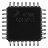
MC908GZ60CFJE Freescale Semiconductor, MC908GZ60CFJE Datasheet - Page 296

MC908GZ60CFJE
Manufacturer Part Number
MC908GZ60CFJE
Description
IC MCU 60K FLASH 8MHZ 32-LQFP
Manufacturer
Freescale Semiconductor
Series
HC08r
Datasheet
1.MC908GZ60CFJE.pdf
(352 pages)
Specifications of MC908GZ60CFJE
Core Processor
HC08
Core Size
8-Bit
Speed
8MHz
Connectivity
CAN, SCI, SPI
Peripherals
LVD, POR, PWM
Number Of I /o
21
Program Memory Size
60KB (60K x 8)
Program Memory Type
FLASH
Ram Size
2K x 8
Voltage - Supply (vcc/vdd)
3 V ~ 5.5 V
Data Converters
A/D 24x10b
Oscillator Type
Internal
Operating Temperature
-40°C ~ 85°C
Package / Case
32-LQFP
Controller Family/series
HC08
No. Of I/o's
21
Ram Memory Size
2KB
Cpu Speed
8MHz
No. Of Timers
2
Embedded Interface Type
CAN, SCI, SPI
Rohs Compliant
Yes
Processor Series
HC08GZ
Core
HC08
Data Bus Width
8 bit
Data Ram Size
2 KB
Interface Type
CAN, ESCI, SPI
Maximum Clock Frequency
8 MHz
Number Of Programmable I/os
53
Number Of Timers
8
Maximum Operating Temperature
+ 85 C
Mounting Style
SMD/SMT
Development Tools By Supplier
FSICEBASE, DEMO908GZ60E, M68EML08GZE
Minimum Operating Temperature
- 40 C
On-chip Adc
10 bit, 24 Channel
Lead Free Status / RoHS Status
Lead free / RoHS Compliant
Eeprom Size
-
Lead Free Status / Rohs Status
Details
Available stocks
Company
Part Number
Manufacturer
Quantity
Price
Company:
Part Number:
MC908GZ60CFJE
Manufacturer:
Freescale
Quantity:
4 000
Company:
Part Number:
MC908GZ60CFJE
Manufacturer:
Freescale Semiconductor
Quantity:
10 000
- Current page: 296 of 352
- Download datasheet (5Mb)
Timer Interface Module (TIM2)
ELSxB and ELSxA — Edge/Level Select Bits
TOVx — Toggle-On-Overflow Bit
CHxMAX — Channel x Maximum Duty Cycle Bit
296
When channel x is an input capture channel, these read/write bits control the active edge-sensing logic
on channel x.
When channel x is an output compare channel, ELSxB and ELSxA control the channel x output
behavior when an output compare occurs.
When ELSxB and ELSxA are both clear, channel x is not connected to port D or port F, and pin
PTDx/T2CHx or pin PTFx/T2CHx is available as a general- purpose I/O pin.
ELSxB and ELSxA work. Reset clears the ELSxB and ELSxA bits.
When channel x is an output compare channel, this read/write bit controls the behavior of the channel
x output when the TIM2 counter overflows. When channel x is an input capture channel, TOVx has no
effect. Reset clears the TOVx bit.
When the TOVx bit is at a 1 and clear output on compare is selected, setting the CHxMAX bit forces
the duty cycle of buffered and unbuffered PWM signals to 100%. As
bit takes effect in the cycle after it is set or cleared. The output stays at 100% duty cycle level until the
cycle after CHxMAX is cleared.
1 = Channel x pin toggles on TIM2 counter overflow.
0 = Channel x pin does not toggle on TIM2 counter overflow.
PTDx/T2CHx
After initially enabling a TIM2 channel register for input capture operation
and selecting the edge sensitivity, clear CHxF to ignore any erroneous
edge detection flags.
When TOVx is set, a TIM2 counter overflow takes precedence over a
channel x output compare if both occur at the same time.
The 100% PWM duty cycle is defined as a continuous high level if the PWM
polarity is 1 and a continuous low level if the PWM polarity is 0. Conversely,
a 0% PWM duty cycle is defined as a continuous low level if the PWM
polarity is 1 and a continuous high level if the PWM polarity is 0.
CHxMAX
MC68HC908GZ60 • MC68HC908GZ48 • MC68HC908GZ32 Data Sheet, Rev. 6
OVERFLOW
COMPARE
PERIOD
OUTPUT
Figure 19-9. CHxMAX Latency
OVERFLOW
COMPARE
OUTPUT
NOTE
NOTE
NOTE
OVERFLOW
COMPARE
OUTPUT
OVERFLOW
Figure 19-9
COMPARE
OUTPUT
Table 19-2
OVERFLOW
shows, the CHxMAX
Freescale Semiconductor
shows how
Related parts for MC908GZ60CFJE
Image
Part Number
Description
Manufacturer
Datasheet
Request
R
Part Number:
Description:
Manufacturer:
Freescale Semiconductor, Inc
Datasheet:
Part Number:
Description:
Manufacturer:
Freescale Semiconductor, Inc
Datasheet:
Part Number:
Description:
Manufacturer:
Freescale Semiconductor, Inc
Datasheet:
Part Number:
Description:
Manufacturer:
Freescale Semiconductor, Inc
Datasheet:
Part Number:
Description:
Manufacturer:
Freescale Semiconductor, Inc
Datasheet:
Part Number:
Description:
Manufacturer:
Freescale Semiconductor, Inc
Datasheet:
Part Number:
Description:
Manufacturer:
Freescale Semiconductor, Inc
Datasheet:
Part Number:
Description:
Manufacturer:
Freescale Semiconductor, Inc
Datasheet:
Part Number:
Description:
Manufacturer:
Freescale Semiconductor, Inc
Datasheet:
Part Number:
Description:
Manufacturer:
Freescale Semiconductor, Inc
Datasheet:
Part Number:
Description:
Manufacturer:
Freescale Semiconductor, Inc
Datasheet:
Part Number:
Description:
Manufacturer:
Freescale Semiconductor, Inc
Datasheet:
Part Number:
Description:
Manufacturer:
Freescale Semiconductor, Inc
Datasheet:
Part Number:
Description:
Manufacturer:
Freescale Semiconductor, Inc
Datasheet:
Part Number:
Description:
Manufacturer:
Freescale Semiconductor, Inc
Datasheet:


