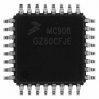
MC908GZ60CFJE Freescale Semiconductor, MC908GZ60CFJE Datasheet - Page 52

MC908GZ60CFJE
Manufacturer Part Number
MC908GZ60CFJE
Description
IC MCU 60K FLASH 8MHZ 32-LQFP
Manufacturer
Freescale Semiconductor
Series
HC08r
Datasheet
1.MC908GZ60CFJE.pdf
(352 pages)
Specifications of MC908GZ60CFJE
Core Processor
HC08
Core Size
8-Bit
Speed
8MHz
Connectivity
CAN, SCI, SPI
Peripherals
LVD, POR, PWM
Number Of I /o
21
Program Memory Size
60KB (60K x 8)
Program Memory Type
FLASH
Ram Size
2K x 8
Voltage - Supply (vcc/vdd)
3 V ~ 5.5 V
Data Converters
A/D 24x10b
Oscillator Type
Internal
Operating Temperature
-40°C ~ 85°C
Package / Case
32-LQFP
Controller Family/series
HC08
No. Of I/o's
21
Ram Memory Size
2KB
Cpu Speed
8MHz
No. Of Timers
2
Embedded Interface Type
CAN, SCI, SPI
Rohs Compliant
Yes
Processor Series
HC08GZ
Core
HC08
Data Bus Width
8 bit
Data Ram Size
2 KB
Interface Type
CAN, ESCI, SPI
Maximum Clock Frequency
8 MHz
Number Of Programmable I/os
53
Number Of Timers
8
Maximum Operating Temperature
+ 85 C
Mounting Style
SMD/SMT
Development Tools By Supplier
FSICEBASE, DEMO908GZ60E, M68EML08GZE
Minimum Operating Temperature
- 40 C
On-chip Adc
10 bit, 24 Channel
Lead Free Status / RoHS Status
Lead free / RoHS Compliant
Eeprom Size
-
Lead Free Status / Rohs Status
Details
Available stocks
Company
Part Number
Manufacturer
Quantity
Price
Company:
Part Number:
MC908GZ60CFJE
Manufacturer:
Freescale
Quantity:
4 000
Company:
Part Number:
MC908GZ60CFJE
Manufacturer:
Freescale Semiconductor
Quantity:
10 000
- Current page: 52 of 352
- Download datasheet (5Mb)
Memory
2.6.7 Low-Power Modes
The WAIT and STOP instructions will place the MCU in low power-consumption standby modes.
2.6.7.1 Wait Mode
Putting the MCU into wait mode while the FLASH is in read mode does not affect the operation of the
FLASH memory directly; however, no memory activity will take place since the CPU is inactive.
The WAIT instruction should not be executed while performing a program or erase operation on the
FLASH. Wait mode will suspend any FLASH program/erase operations and leave the memory in a
standby mode.
2.6.7.2 Stop Mode
Putting the MCU into stop mode while the FLASH is in read mode does not affect the operation of the
FLASH memory directly; however, no memory activity will take place since the CPU is inactive.
The STOP instruction should not be executed while performing a program or erase operation on the
FLASH. Stop mode will suspend any FLASH program/erase operations and leave the memory in a
standby mode.
2.7 FLASH-2 Memory (FLASH-2)
This subsection describes the operation of the embedded FLASH-2 memory. This memory can be read,
programmed, and erased from a single external supply. The program and erase operations are enabled
through the use of an internal charge pump.
2.7.1 Functional Description
The FLASH-2 memory is a non-continuous array consisting of a total of 29,822 bytes. An erased bit reads
as a 1 and a programmed bit reads as a 0.
Memory in the FLASH-2 array is organized into rows within pages. There are two rows of memory per
page with 64 bytes per row. The minimum erase block size is a single page,128 bytes. Programming is
performed on a per-row basis, 64 bytes at a time. Program and erase operations are facilitated through
control bits in the FLASH-2 control register (FL2CR). Details for these operations appear later in this
subsection.
The FLASH-2 memory map consists of:
52
•
•
•
•
•
$0462–$04FF: user memory (158 bytes)
$0980–$1B7F: user memory (4608 bytes)
$1E20–$7FFF: user memory (25056 bytes)
$FF81: FLASH-2 block protect register (FL2BPR)
$FE08: FLASH-2 control register (FL2CR)
Standby mode is the power saving mode of the FLASH module, in which all
internal control signals to the FLASH are inactive and the current
consumption of the FLASH is minimum.
FL2BPR physically resides within FLASH-1 memory addressing space
MC68HC908GZ60 • MC68HC908GZ48 • MC68HC908GZ32 Data Sheet, Rev. 6
NOTE
NOTE
Freescale Semiconductor
Related parts for MC908GZ60CFJE
Image
Part Number
Description
Manufacturer
Datasheet
Request
R
Part Number:
Description:
Manufacturer:
Freescale Semiconductor, Inc
Datasheet:
Part Number:
Description:
Manufacturer:
Freescale Semiconductor, Inc
Datasheet:
Part Number:
Description:
Manufacturer:
Freescale Semiconductor, Inc
Datasheet:
Part Number:
Description:
Manufacturer:
Freescale Semiconductor, Inc
Datasheet:
Part Number:
Description:
Manufacturer:
Freescale Semiconductor, Inc
Datasheet:
Part Number:
Description:
Manufacturer:
Freescale Semiconductor, Inc
Datasheet:
Part Number:
Description:
Manufacturer:
Freescale Semiconductor, Inc
Datasheet:
Part Number:
Description:
Manufacturer:
Freescale Semiconductor, Inc
Datasheet:
Part Number:
Description:
Manufacturer:
Freescale Semiconductor, Inc
Datasheet:
Part Number:
Description:
Manufacturer:
Freescale Semiconductor, Inc
Datasheet:
Part Number:
Description:
Manufacturer:
Freescale Semiconductor, Inc
Datasheet:
Part Number:
Description:
Manufacturer:
Freescale Semiconductor, Inc
Datasheet:
Part Number:
Description:
Manufacturer:
Freescale Semiconductor, Inc
Datasheet:
Part Number:
Description:
Manufacturer:
Freescale Semiconductor, Inc
Datasheet:
Part Number:
Description:
Manufacturer:
Freescale Semiconductor, Inc
Datasheet:


