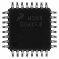
MC908GZ60CFJE Freescale Semiconductor, MC908GZ60CFJE Datasheet - Page 67

MC908GZ60CFJE
Manufacturer Part Number
MC908GZ60CFJE
Description
IC MCU 60K FLASH 8MHZ 32-LQFP
Manufacturer
Freescale Semiconductor
Series
HC08r
Datasheet
1.MC908GZ60CFJE.pdf
(352 pages)
Specifications of MC908GZ60CFJE
Core Processor
HC08
Core Size
8-Bit
Speed
8MHz
Connectivity
CAN, SCI, SPI
Peripherals
LVD, POR, PWM
Number Of I /o
21
Program Memory Size
60KB (60K x 8)
Program Memory Type
FLASH
Ram Size
2K x 8
Voltage - Supply (vcc/vdd)
3 V ~ 5.5 V
Data Converters
A/D 24x10b
Oscillator Type
Internal
Operating Temperature
-40°C ~ 85°C
Package / Case
32-LQFP
Controller Family/series
HC08
No. Of I/o's
21
Ram Memory Size
2KB
Cpu Speed
8MHz
No. Of Timers
2
Embedded Interface Type
CAN, SCI, SPI
Rohs Compliant
Yes
Processor Series
HC08GZ
Core
HC08
Data Bus Width
8 bit
Data Ram Size
2 KB
Interface Type
CAN, ESCI, SPI
Maximum Clock Frequency
8 MHz
Number Of Programmable I/os
53
Number Of Timers
8
Maximum Operating Temperature
+ 85 C
Mounting Style
SMD/SMT
Development Tools By Supplier
FSICEBASE, DEMO908GZ60E, M68EML08GZE
Minimum Operating Temperature
- 40 C
On-chip Adc
10 bit, 24 Channel
Lead Free Status / RoHS Status
Lead free / RoHS Compliant
Eeprom Size
-
Lead Free Status / Rohs Status
Details
Available stocks
Company
Part Number
Manufacturer
Quantity
Price
Company:
Part Number:
MC908GZ60CFJE
Manufacturer:
Freescale
Quantity:
4 000
Company:
Part Number:
MC908GZ60CFJE
Manufacturer:
Freescale Semiconductor
Quantity:
10 000
- Current page: 67 of 352
- Download datasheet (5Mb)
3.7.3 ADC Voltage Reference High Pin (V
The ADC analog portion uses V
pin to the same voltage potential as V
good results. Any noise present on this pin will be reflected and possibly magnified in A/D conversion
values.
V
3.7.4 ADC Voltage Reference Low Pin (V
The ADC analog portion uses V
to the same voltage potential as V
results. Any noise present on this pin will be reflected and possibly magnified in A/D conversion values.
V
3.7.5 ADC Voltage In (V
V
3.8 I/O Registers
These I/O registers control and monitor ADC operation:
Freescale Semiconductor
DDAD
SSAD
ADIN
•
•
•
is the input voltage signal from one of the 24 ADC channels to the ADC module.
ADC status and control register (ADSCR)
ADC data register (ADRH and ADRL)
ADC clock register (ADCLK)
and V
and V
REFL
REFH
For maximum noise immunity, route V
capacitors as close as possible to the package. Routing V
parallel to V
For maximum noise immunity, route V
to V
Routing V
noise rejection.
are bonded internally.
are bonded internally.
SS
MC68HC908GZ60 • MC68HC908GZ48 • MC68HC908GZ32 Data Sheet, Rev. 6
, place bypass capacitors as close as possible to the package.
REFH
REFL
ADIN
close and parallel to V
REFL
REFH
may improve common mode noise rejection.
)
SS
. External filtering is often necessary to ensure a clean V
as its lower voltage reference pin. By default, connect the V
DD
as its upper voltage reference pin. By default, connect the V
. External filtering is often necessary to ensure a clean V
REFL
REFH
NOTE
NOTE
REFL
REFH
)
REFL
)
may improve common mode
carefully and, if not connected
carefully and place bypass
REFH
close and
REFL
I/O Registers
REFH
REFL
for good
REFH
pin
for
67
Related parts for MC908GZ60CFJE
Image
Part Number
Description
Manufacturer
Datasheet
Request
R
Part Number:
Description:
Manufacturer:
Freescale Semiconductor, Inc
Datasheet:
Part Number:
Description:
Manufacturer:
Freescale Semiconductor, Inc
Datasheet:
Part Number:
Description:
Manufacturer:
Freescale Semiconductor, Inc
Datasheet:
Part Number:
Description:
Manufacturer:
Freescale Semiconductor, Inc
Datasheet:
Part Number:
Description:
Manufacturer:
Freescale Semiconductor, Inc
Datasheet:
Part Number:
Description:
Manufacturer:
Freescale Semiconductor, Inc
Datasheet:
Part Number:
Description:
Manufacturer:
Freescale Semiconductor, Inc
Datasheet:
Part Number:
Description:
Manufacturer:
Freescale Semiconductor, Inc
Datasheet:
Part Number:
Description:
Manufacturer:
Freescale Semiconductor, Inc
Datasheet:
Part Number:
Description:
Manufacturer:
Freescale Semiconductor, Inc
Datasheet:
Part Number:
Description:
Manufacturer:
Freescale Semiconductor, Inc
Datasheet:
Part Number:
Description:
Manufacturer:
Freescale Semiconductor, Inc
Datasheet:
Part Number:
Description:
Manufacturer:
Freescale Semiconductor, Inc
Datasheet:
Part Number:
Description:
Manufacturer:
Freescale Semiconductor, Inc
Datasheet:
Part Number:
Description:
Manufacturer:
Freescale Semiconductor, Inc
Datasheet:


