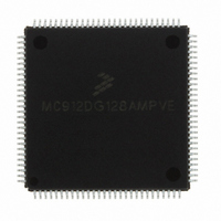
MC912DG128AMPVE Freescale Semiconductor, MC912DG128AMPVE Datasheet - Page 120

MC912DG128AMPVE
Manufacturer Part Number
MC912DG128AMPVE
Description
IC MCU 128K FLASH 8MHZ 112-LQFP
Manufacturer
Freescale Semiconductor
Series
HC12r
Datasheet
1.MC912DG128ACPVER.pdf
(478 pages)
Specifications of MC912DG128AMPVE
Core Processor
CPU12
Core Size
16-Bit
Speed
8MHz
Connectivity
CAN, I²C, SCI, SPI
Peripherals
POR, PWM, WDT
Number Of I /o
69
Program Memory Size
128KB (128K x 8)
Program Memory Type
FLASH
Eeprom Size
2K x 8
Ram Size
8K x 8
Voltage - Supply (vcc/vdd)
4.5 V ~ 5.5 V
Data Converters
A/D 16x8/10b
Oscillator Type
Internal
Operating Temperature
-40°C ~ 125°C
Package / Case
112-LQFP
Processor Series
HC912D
Core
HC12
Data Bus Width
16 bit
Data Ram Size
8 KB
Interface Type
CAN/I2C/SCI/SPI
Maximum Clock Frequency
8 MHz
Number Of Programmable I/os
69
Number Of Timers
8
Maximum Operating Temperature
+ 125 C
Mounting Style
SMD/SMT
3rd Party Development Tools
EWHCS12
Minimum Operating Temperature
- 40 C
On-chip Adc
2 (8-ch x 10-bit)
Lead Free Status / RoHS Status
Lead free / RoHS Compliant
Available stocks
Company
Part Number
Manufacturer
Quantity
Price
Company:
Part Number:
MC912DG128AMPVE
Manufacturer:
FREESCALE
Quantity:
2 902
Company:
Part Number:
MC912DG128AMPVE
Manufacturer:
Freescale Semiconductor
Quantity:
10 000
- Current page: 120 of 478
- Download datasheet (4Mb)
Flash Memory
8.8 Programming the Flash EEPROM
Technical Data
120
Programming and erasing of Flash locations cannot be performed by
code being executed from the Flash memory. While these operations
must be performed in the order shown, other unrelated operations may
occur between the steps. Do not exceed t
Programming the Flash EEPROM is done on a row basis. A row consists
of 32 consecutive words (64 bytes) with rows starting from addresses
$XX00, $XX40, $XX80 and $XXC0. When writing a row care should be
taken not to write data to addresses outside of the row. Programming is
restricted to aligned word i.e. data writes to select rows/blocks for
programming/erase should be to even adresses and writes to any row
for programming should be to aligned words.
Use this step-by-step procedure to program a row of Flash memory.
10. Wait for a time, t
11. Clear the HVEN bit.
1. Set the PGM bit. This configures the memory for program
2. Write to any aligned word Flash address within the row address
3. Wait for a time, t
4. Set the HVEN bit.
5. Wait for a time, t
6. Write one data word (two bytes) to the next aligned word Flash
7. Wait for a time, t
8. Repeat step 6 and 7 until all the words within the row are
9. Clear the PGM bit.
Freescale Semiconductor, Inc.
For More Information On This Product,
operation and enables the latching of address and data for
programming.
range desired (with any data) to select the row.
address to be programmed. If BOOTP is asserted, an attempt to
program an address in the boot block will be ignored.
programmed.
Go to: www.freescale.com
Flash Memory
NVS
PGS
FPGM
NVH
(min. 10µs).
(min. 5µs).
(min. 5µs).
(min. 30µs).
FPGM
MC68HC912DT128A — Rev 4.0
maximum (40µs).
MOTOROLA
Related parts for MC912DG128AMPVE
Image
Part Number
Description
Manufacturer
Datasheet
Request
R
Part Number:
Description:
Manufacturer:
Freescale Semiconductor, Inc
Datasheet:
Part Number:
Description:
Manufacturer:
Freescale Semiconductor, Inc
Datasheet:
Part Number:
Description:
Manufacturer:
Freescale Semiconductor, Inc
Datasheet:
Part Number:
Description:
Manufacturer:
Freescale Semiconductor, Inc
Datasheet:
Part Number:
Description:
Manufacturer:
Freescale Semiconductor, Inc
Datasheet:
Part Number:
Description:
Manufacturer:
Freescale Semiconductor, Inc
Datasheet:
Part Number:
Description:
Manufacturer:
Freescale Semiconductor, Inc
Datasheet:
Part Number:
Description:
Manufacturer:
Freescale Semiconductor, Inc
Datasheet:
Part Number:
Description:
Manufacturer:
Freescale Semiconductor, Inc
Datasheet:
Part Number:
Description:
Manufacturer:
Freescale Semiconductor, Inc
Datasheet:
Part Number:
Description:
Manufacturer:
Freescale Semiconductor, Inc
Datasheet:
Part Number:
Description:
Manufacturer:
Freescale Semiconductor, Inc
Datasheet:
Part Number:
Description:
Manufacturer:
Freescale Semiconductor, Inc
Datasheet:
Part Number:
Description:
Manufacturer:
Freescale Semiconductor, Inc
Datasheet:
Part Number:
Description:
Manufacturer:
Freescale Semiconductor, Inc
Datasheet:


