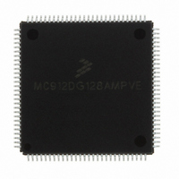
MC912DG128AMPVE Freescale Semiconductor, MC912DG128AMPVE Datasheet - Page 125

MC912DG128AMPVE
Manufacturer Part Number
MC912DG128AMPVE
Description
IC MCU 128K FLASH 8MHZ 112-LQFP
Manufacturer
Freescale Semiconductor
Series
HC12r
Datasheet
1.MC912DG128ACPVER.pdf
(478 pages)
Specifications of MC912DG128AMPVE
Core Processor
CPU12
Core Size
16-Bit
Speed
8MHz
Connectivity
CAN, I²C, SCI, SPI
Peripherals
POR, PWM, WDT
Number Of I /o
69
Program Memory Size
128KB (128K x 8)
Program Memory Type
FLASH
Eeprom Size
2K x 8
Ram Size
8K x 8
Voltage - Supply (vcc/vdd)
4.5 V ~ 5.5 V
Data Converters
A/D 16x8/10b
Oscillator Type
Internal
Operating Temperature
-40°C ~ 125°C
Package / Case
112-LQFP
Processor Series
HC912D
Core
HC12
Data Bus Width
16 bit
Data Ram Size
8 KB
Interface Type
CAN/I2C/SCI/SPI
Maximum Clock Frequency
8 MHz
Number Of Programmable I/os
69
Number Of Timers
8
Maximum Operating Temperature
+ 125 C
Mounting Style
SMD/SMT
3rd Party Development Tools
EWHCS12
Minimum Operating Temperature
- 40 C
On-chip Adc
2 (8-ch x 10-bit)
Lead Free Status / RoHS Status
Lead free / RoHS Compliant
Available stocks
Company
Part Number
Manufacturer
Quantity
Price
Company:
Part Number:
MC912DG128AMPVE
Manufacturer:
FREESCALE
Quantity:
2 902
Company:
Part Number:
MC912DG128AMPVE
Manufacturer:
Freescale Semiconductor
Quantity:
10 000
- Current page: 125 of 478
- Download datasheet (4Mb)
9.4 EEPROM Programmer’s Model
MC68HC912DT128A — Rev 4.0
MOTOROLA
CAUTION:
The EEPROM module consists of two separately addressable sections.
The first is an eight-byte memory mapped control register block used for
control, testing and configuration of the EEPROM array. The second
section is the EEPROM array itself.
At reset, the eight-byte register section starts at address $00EC and the
EEPROM array is located from addresses $0800 to $0FFF. Registers
$00EC-$00ED are reserved.
Read/write access to the memory array section can be enabled or
disabled by the EEON control bit in the INITEE register ($0012). This
feature allows the access of memory mapped resources that have lower
priority than the EEPROM memory array. EEPROM control registers can
be accessed regardless of the state of EEON. Any EEPROM erase or
program operation already in progress will not be affected by the change
of EEON state. For information on re-mapping the register block and
EEPROM address space, refer to
It is strongly recommended to discontinue program/erase operations
during WAIT (when EESWAI=1) or STOP modes since all
program/erase activities will be terminated abruptly and considered
unsuccessful.
For lowest power consumption during WAIT mode, it is advised to turn
off EEPGM.
The EEPROM module contains an extra word called SHADOW word
which is loaded at reset into the EEMCR, EEDIVH and EEDIVL
registers. To program the SHADOW word, when in special modes
(SMODN=0), the NOSHW bit in EEMCR register must be cleared.
Normal programming routines are used to program the SHADOW word
which becomes accessible at address $0FC0-$0FC1 when NOSHW is
cleared. At the next reset the SHADOW word data is loaded into the
EEMCR, EEDIVH and EEDIVL registers. The SHADOW word can be
protected from being programmed or erased by setting the SHPROT bit
of EEPROT register.
Freescale Semiconductor, Inc.
For More Information On This Product,
Go to: www.freescale.com
EEPROM Memory
Operating
Modes.
EEPROM Programmer’s Model
EEPROM Memory
Technical Data
125
Related parts for MC912DG128AMPVE
Image
Part Number
Description
Manufacturer
Datasheet
Request
R
Part Number:
Description:
Manufacturer:
Freescale Semiconductor, Inc
Datasheet:
Part Number:
Description:
Manufacturer:
Freescale Semiconductor, Inc
Datasheet:
Part Number:
Description:
Manufacturer:
Freescale Semiconductor, Inc
Datasheet:
Part Number:
Description:
Manufacturer:
Freescale Semiconductor, Inc
Datasheet:
Part Number:
Description:
Manufacturer:
Freescale Semiconductor, Inc
Datasheet:
Part Number:
Description:
Manufacturer:
Freescale Semiconductor, Inc
Datasheet:
Part Number:
Description:
Manufacturer:
Freescale Semiconductor, Inc
Datasheet:
Part Number:
Description:
Manufacturer:
Freescale Semiconductor, Inc
Datasheet:
Part Number:
Description:
Manufacturer:
Freescale Semiconductor, Inc
Datasheet:
Part Number:
Description:
Manufacturer:
Freescale Semiconductor, Inc
Datasheet:
Part Number:
Description:
Manufacturer:
Freescale Semiconductor, Inc
Datasheet:
Part Number:
Description:
Manufacturer:
Freescale Semiconductor, Inc
Datasheet:
Part Number:
Description:
Manufacturer:
Freescale Semiconductor, Inc
Datasheet:
Part Number:
Description:
Manufacturer:
Freescale Semiconductor, Inc
Datasheet:
Part Number:
Description:
Manufacturer:
Freescale Semiconductor, Inc
Datasheet:


