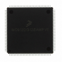
MC912DG128AMPVE Freescale Semiconductor, MC912DG128AMPVE Datasheet - Page 146

MC912DG128AMPVE
Manufacturer Part Number
MC912DG128AMPVE
Description
IC MCU 128K FLASH 8MHZ 112-LQFP
Manufacturer
Freescale Semiconductor
Series
HC12r
Datasheet
1.MC912DG128ACPVER.pdf
(478 pages)
Specifications of MC912DG128AMPVE
Core Processor
CPU12
Core Size
16-Bit
Speed
8MHz
Connectivity
CAN, I²C, SCI, SPI
Peripherals
POR, PWM, WDT
Number Of I /o
69
Program Memory Size
128KB (128K x 8)
Program Memory Type
FLASH
Eeprom Size
2K x 8
Ram Size
8K x 8
Voltage - Supply (vcc/vdd)
4.5 V ~ 5.5 V
Data Converters
A/D 16x8/10b
Oscillator Type
Internal
Operating Temperature
-40°C ~ 125°C
Package / Case
112-LQFP
Processor Series
HC912D
Core
HC12
Data Bus Width
16 bit
Data Ram Size
8 KB
Interface Type
CAN/I2C/SCI/SPI
Maximum Clock Frequency
8 MHz
Number Of Programmable I/os
69
Number Of Timers
8
Maximum Operating Temperature
+ 125 C
Mounting Style
SMD/SMT
3rd Party Development Tools
EWHCS12
Minimum Operating Temperature
- 40 C
On-chip Adc
2 (8-ch x 10-bit)
Lead Free Status / RoHS Status
Lead free / RoHS Compliant
Available stocks
Company
Part Number
Manufacturer
Quantity
Price
Company:
Part Number:
MC912DG128AMPVE
Manufacturer:
FREESCALE
Quantity:
2 902
Company:
Part Number:
MC912DG128AMPVE
Manufacturer:
Freescale Semiconductor
Quantity:
10 000
- Current page: 146 of 478
- Download datasheet (4Mb)
Resets and Interrupts
10.9.3 Interrupts
10.9.4 Parallel I/O
10.9.5 Central Processing Unit
10.9.6 Memory
Technical Data
146
PSEL is initialized in the HPRIO register with the value $F2, causing the
external IRQ pin to have the highest I-bit interrupt priority. The IRQ pin
is configured for level-sensitive operation (for wired-OR systems).
However, the interrupt mask bits in the CPU12 CCR are set to mask X-
and I-related interrupt requests.
If the MCU comes out of reset in a single-chip mode, all ports are
configured as general-purpose high-impedance inputs.
If the MCU comes out of reset in an expanded mode, port A and port B
are used for the address/data bus, and port E pins are normally used to
control the external bus (operation of port E pins can be affected by the
PEAR register). Out of reset, port J, port H, port K, port IB, port P, port
S, port T, port AD0 and port AD1 are all configured as general-purpose
inputs.
After reset, the CPU fetches a vector from the appropriate address, then
begins executing instructions. The stack pointer and other CPU registers
are indeterminate immediately after reset. The CCR X and I interrupt
mask bits are set to mask any interrupt requests. The S bit is also set to
inhibit the STOP instruction.
After reset, the internal register block is located from $0000 to $03FF,
RAM is at $2000 to $3FFF, and EEPROM is located at $0800 to $0FFF.
In single chip mode one 32-Kbyte FLASH EEPROM module is located
from $4000 to $7FFF and $C000 to $FFFF, and the other three 32-Kbyte
FLASH EEPROM modules are accessible through the program page
window located from $8000 to $BFFF. The first 32-Kbyte FLASH
EEPROM is also accessible through the program page window.
Freescale Semiconductor, Inc.
For More Information On This Product,
Go to: www.freescale.com
Resets and Interrupts
MC68HC912DT128A — Rev 4.0
MOTOROLA
Related parts for MC912DG128AMPVE
Image
Part Number
Description
Manufacturer
Datasheet
Request
R
Part Number:
Description:
Manufacturer:
Freescale Semiconductor, Inc
Datasheet:
Part Number:
Description:
Manufacturer:
Freescale Semiconductor, Inc
Datasheet:
Part Number:
Description:
Manufacturer:
Freescale Semiconductor, Inc
Datasheet:
Part Number:
Description:
Manufacturer:
Freescale Semiconductor, Inc
Datasheet:
Part Number:
Description:
Manufacturer:
Freescale Semiconductor, Inc
Datasheet:
Part Number:
Description:
Manufacturer:
Freescale Semiconductor, Inc
Datasheet:
Part Number:
Description:
Manufacturer:
Freescale Semiconductor, Inc
Datasheet:
Part Number:
Description:
Manufacturer:
Freescale Semiconductor, Inc
Datasheet:
Part Number:
Description:
Manufacturer:
Freescale Semiconductor, Inc
Datasheet:
Part Number:
Description:
Manufacturer:
Freescale Semiconductor, Inc
Datasheet:
Part Number:
Description:
Manufacturer:
Freescale Semiconductor, Inc
Datasheet:
Part Number:
Description:
Manufacturer:
Freescale Semiconductor, Inc
Datasheet:
Part Number:
Description:
Manufacturer:
Freescale Semiconductor, Inc
Datasheet:
Part Number:
Description:
Manufacturer:
Freescale Semiconductor, Inc
Datasheet:
Part Number:
Description:
Manufacturer:
Freescale Semiconductor, Inc
Datasheet:


