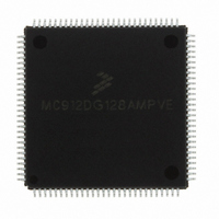
MC912DG128AMPVE Freescale Semiconductor, MC912DG128AMPVE Datasheet - Page 298

MC912DG128AMPVE
Manufacturer Part Number
MC912DG128AMPVE
Description
IC MCU 128K FLASH 8MHZ 112-LQFP
Manufacturer
Freescale Semiconductor
Series
HC12r
Datasheet
1.MC912DG128ACPVER.pdf
(478 pages)
Specifications of MC912DG128AMPVE
Core Processor
CPU12
Core Size
16-Bit
Speed
8MHz
Connectivity
CAN, I²C, SCI, SPI
Peripherals
POR, PWM, WDT
Number Of I /o
69
Program Memory Size
128KB (128K x 8)
Program Memory Type
FLASH
Eeprom Size
2K x 8
Ram Size
8K x 8
Voltage - Supply (vcc/vdd)
4.5 V ~ 5.5 V
Data Converters
A/D 16x8/10b
Oscillator Type
Internal
Operating Temperature
-40°C ~ 125°C
Package / Case
112-LQFP
Processor Series
HC912D
Core
HC12
Data Bus Width
16 bit
Data Ram Size
8 KB
Interface Type
CAN/I2C/SCI/SPI
Maximum Clock Frequency
8 MHz
Number Of Programmable I/os
69
Number Of Timers
8
Maximum Operating Temperature
+ 125 C
Mounting Style
SMD/SMT
3rd Party Development Tools
EWHCS12
Minimum Operating Temperature
- 40 C
On-chip Adc
2 (8-ch x 10-bit)
Lead Free Status / RoHS Status
Lead free / RoHS Compliant
Available stocks
Company
Part Number
Manufacturer
Quantity
Price
Company:
Part Number:
MC912DG128AMPVE
Manufacturer:
FREESCALE
Quantity:
2 902
Company:
Part Number:
MC912DG128AMPVE
Manufacturer:
Freescale Semiconductor
Quantity:
10 000
- Current page: 298 of 478
- Download datasheet (4Mb)
SP0DR — SPI Data Register
Multiple Serial Interface
Technical Data
298
Bit 7
Bit 7
6
6
WCOL — Write Collision Status Flag
MODF — SPI Mode Error Interrupt Status Flag
Read anytime (normally only after SPIF flag set). Write anytime (see
WCOL write collision flag).
Reset does not affect this address.
This 8-bit register is both the input and output register for SPI data.
Reads of this register are double buffered but writes cause data to
written directly into the serial shifter. In the SPI system the 8-bit data
register in the master and the 8-bit data register in the slave are linked
by the MOSI and MISO wires to form a distributed 16-bit register. When
a data transfer operation is performed, this 16-bit register is serially
shifted eight bit positions by the SCK clock from the master so the data
is effectively exchanged between the master and the slave. Note that
The MCU write is disabled to avoid writing over the data being
transferred. No interrupt is generated because the error status flag
can be read upon completion of the transfer that was in progress at
the time of the error. Automatically cleared by a read of the SP0SR
(with WCOL set) followed by an access (read or write) to the SP0DR
register.
This bit is set automatically by SPI hardware if the MSTR control bit is
set and the slave select input pin becomes zero. This condition is not
permitted in normal operation. In the case where DDRS bit 7 is set,
the PS7 pin is a general-purpose output pin or SS output pin rather
than being dedicated as the SS input for the SPI system. In this
special case the mode fault function is inhibited and MODF remains
cleared. This flag is automatically cleared by a read of the SP0SR
(with MODF set) followed by a write to the SP0CR1 register.
Freescale Semiconductor, Inc.
For More Information On This Product,
0 = No write collision
1 = Indicates that a serial transfer was in progress when the MCU
5
5
tried to write new data into the SP0DR data register.
Go to: www.freescale.com
Multiple Serial Interface
4
4
3
3
2
2
MC68HC912DT128A — Rev 4.0
1
1
Bit 0
Bit 0
MOTOROLA
$00D5
Related parts for MC912DG128AMPVE
Image
Part Number
Description
Manufacturer
Datasheet
Request
R
Part Number:
Description:
Manufacturer:
Freescale Semiconductor, Inc
Datasheet:
Part Number:
Description:
Manufacturer:
Freescale Semiconductor, Inc
Datasheet:
Part Number:
Description:
Manufacturer:
Freescale Semiconductor, Inc
Datasheet:
Part Number:
Description:
Manufacturer:
Freescale Semiconductor, Inc
Datasheet:
Part Number:
Description:
Manufacturer:
Freescale Semiconductor, Inc
Datasheet:
Part Number:
Description:
Manufacturer:
Freescale Semiconductor, Inc
Datasheet:
Part Number:
Description:
Manufacturer:
Freescale Semiconductor, Inc
Datasheet:
Part Number:
Description:
Manufacturer:
Freescale Semiconductor, Inc
Datasheet:
Part Number:
Description:
Manufacturer:
Freescale Semiconductor, Inc
Datasheet:
Part Number:
Description:
Manufacturer:
Freescale Semiconductor, Inc
Datasheet:
Part Number:
Description:
Manufacturer:
Freescale Semiconductor, Inc
Datasheet:
Part Number:
Description:
Manufacturer:
Freescale Semiconductor, Inc
Datasheet:
Part Number:
Description:
Manufacturer:
Freescale Semiconductor, Inc
Datasheet:
Part Number:
Description:
Manufacturer:
Freescale Semiconductor, Inc
Datasheet:
Part Number:
Description:
Manufacturer:
Freescale Semiconductor, Inc
Datasheet:


