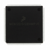
MC912DG128AMPVE Freescale Semiconductor, MC912DG128AMPVE Datasheet - Page 49

MC912DG128AMPVE
Manufacturer Part Number
MC912DG128AMPVE
Description
IC MCU 128K FLASH 8MHZ 112-LQFP
Manufacturer
Freescale Semiconductor
Series
HC12r
Datasheet
1.MC912DG128ACPVER.pdf
(478 pages)
Specifications of MC912DG128AMPVE
Core Processor
CPU12
Core Size
16-Bit
Speed
8MHz
Connectivity
CAN, I²C, SCI, SPI
Peripherals
POR, PWM, WDT
Number Of I /o
69
Program Memory Size
128KB (128K x 8)
Program Memory Type
FLASH
Eeprom Size
2K x 8
Ram Size
8K x 8
Voltage - Supply (vcc/vdd)
4.5 V ~ 5.5 V
Data Converters
A/D 16x8/10b
Oscillator Type
Internal
Operating Temperature
-40°C ~ 125°C
Package / Case
112-LQFP
Processor Series
HC912D
Core
HC12
Data Bus Width
16 bit
Data Ram Size
8 KB
Interface Type
CAN/I2C/SCI/SPI
Maximum Clock Frequency
8 MHz
Number Of Programmable I/os
69
Number Of Timers
8
Maximum Operating Temperature
+ 125 C
Mounting Style
SMD/SMT
3rd Party Development Tools
EWHCS12
Minimum Operating Temperature
- 40 C
On-chip Adc
2 (8-ch x 10-bit)
Lead Free Status / RoHS Status
Lead free / RoHS Compliant
Available stocks
Company
Part Number
Manufacturer
Quantity
Price
Company:
Part Number:
MC912DG128AMPVE
Manufacturer:
FREESCALE
Quantity:
2 902
Company:
Part Number:
MC912DG128AMPVE
Manufacturer:
Freescale Semiconductor
Quantity:
10 000
- Current page: 49 of 478
- Download datasheet (4Mb)
MC68HC912DT128A — Rev 4.0
MOTOROLA
output to indicate that an internal failure has been detected in either the
clock monitor or COP watchdog circuit. The MCU goes into reset
asynchronously and comes out of reset synchronously. This allows the
part to reach a proper reset state even if the clocks have failed, while
allowing synchronized operation when starting out of reset.
It is important to use an external low-voltage reset circuit (such as
MC34064 or MC34164) to prevent corruption of RAM or EEPROM due
to power transitions.
The reset sequence is initiated by any of the following events:
External circuitry connected to the reset pin should not include a large
capacitance that would interfere with the ability of this signal to rise to a
valid logic one within nine bus cycles after the low drive is released.
Upon detection of any reset, an internal circuit drives the reset pin low
and a clocked reset sequence controls when the MCU can begin normal
processing. In the case of POR or a clock monitor error, a 4096 cycle
oscillator startup delay is imposed before the reset recovery sequence
starts (reset is driven low throughout this 4096 cycle delay). The internal
reset recovery sequence then drives reset low for 16 to 17 cycles and
releases the drive to allow reset to rise. Nine cycles later this circuit
samples the reset pin to see if it has risen to a logic one level. If reset is
low at this point, the reset is assumed to be coming from an external
request and the internally latched states of the COP timeout and clock
monitor failure are cleared so the normal reset vector ($FFFE:FFFF) is
taken when reset is finally released. If reset is high after this nine cycle
delay, the reset source is tentatively assumed to be either a COP failure
or a clock monitor fail. If the internally latched state of the clock monitor
fail circuit is true, processing begins by fetching the clock monitor vector
($FFFC:FFFD). If no clock monitor failure is indicated, and the latched
state of the COP timeout is true, processing begins by fetching the COP
•
•
•
•
Freescale Semiconductor, Inc.
For More Information On This Product,
Power-on-reset (POR)
COP watchdog enabled and watchdog timer times out
Clock monitor enabled and Clock monitor detects slow or stopped
clock
User applies a low level to the reset pin
Pinout and Signal Descriptions
Go to: www.freescale.com
Pinout and Signal Descriptions
Signal Descriptions
Technical Data
49
Related parts for MC912DG128AMPVE
Image
Part Number
Description
Manufacturer
Datasheet
Request
R
Part Number:
Description:
Manufacturer:
Freescale Semiconductor, Inc
Datasheet:
Part Number:
Description:
Manufacturer:
Freescale Semiconductor, Inc
Datasheet:
Part Number:
Description:
Manufacturer:
Freescale Semiconductor, Inc
Datasheet:
Part Number:
Description:
Manufacturer:
Freescale Semiconductor, Inc
Datasheet:
Part Number:
Description:
Manufacturer:
Freescale Semiconductor, Inc
Datasheet:
Part Number:
Description:
Manufacturer:
Freescale Semiconductor, Inc
Datasheet:
Part Number:
Description:
Manufacturer:
Freescale Semiconductor, Inc
Datasheet:
Part Number:
Description:
Manufacturer:
Freescale Semiconductor, Inc
Datasheet:
Part Number:
Description:
Manufacturer:
Freescale Semiconductor, Inc
Datasheet:
Part Number:
Description:
Manufacturer:
Freescale Semiconductor, Inc
Datasheet:
Part Number:
Description:
Manufacturer:
Freescale Semiconductor, Inc
Datasheet:
Part Number:
Description:
Manufacturer:
Freescale Semiconductor, Inc
Datasheet:
Part Number:
Description:
Manufacturer:
Freescale Semiconductor, Inc
Datasheet:
Part Number:
Description:
Manufacturer:
Freescale Semiconductor, Inc
Datasheet:
Part Number:
Description:
Manufacturer:
Freescale Semiconductor, Inc
Datasheet:


