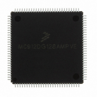
MC912DG128AMPVE Freescale Semiconductor, MC912DG128AMPVE Datasheet - Page 52

MC912DG128AMPVE
Manufacturer Part Number
MC912DG128AMPVE
Description
IC MCU 128K FLASH 8MHZ 112-LQFP
Manufacturer
Freescale Semiconductor
Series
HC12r
Datasheet
1.MC912DG128ACPVER.pdf
(478 pages)
Specifications of MC912DG128AMPVE
Core Processor
CPU12
Core Size
16-Bit
Speed
8MHz
Connectivity
CAN, I²C, SCI, SPI
Peripherals
POR, PWM, WDT
Number Of I /o
69
Program Memory Size
128KB (128K x 8)
Program Memory Type
FLASH
Eeprom Size
2K x 8
Ram Size
8K x 8
Voltage - Supply (vcc/vdd)
4.5 V ~ 5.5 V
Data Converters
A/D 16x8/10b
Oscillator Type
Internal
Operating Temperature
-40°C ~ 125°C
Package / Case
112-LQFP
Processor Series
HC912D
Core
HC12
Data Bus Width
16 bit
Data Ram Size
8 KB
Interface Type
CAN/I2C/SCI/SPI
Maximum Clock Frequency
8 MHz
Number Of Programmable I/os
69
Number Of Timers
8
Maximum Operating Temperature
+ 125 C
Mounting Style
SMD/SMT
3rd Party Development Tools
EWHCS12
Minimum Operating Temperature
- 40 C
On-chip Adc
2 (8-ch x 10-bit)
Lead Free Status / RoHS Status
Lead free / RoHS Compliant
Available stocks
Company
Part Number
Manufacturer
Quantity
Price
Company:
Part Number:
MC912DG128AMPVE
Manufacturer:
FREESCALE
Quantity:
2 902
Company:
Part Number:
MC912DG128AMPVE
Manufacturer:
Freescale Semiconductor
Quantity:
10 000
- Current page: 52 of 478
- Download datasheet (4Mb)
Pinout and Signal Descriptions
3.4.8 External Address and Data Buses (ADDR[15:0] and DATA[15:0])
3.4.9 Read/Write (R/W)
3.4.10 Low-Byte Strobe (LSTRB)
Technical Data
52
External bus pins share functions with general-purpose I/O ports A and
B. In single-chip operating modes, the pins can be used for I/O; in
expanded modes, the pins are used for the external buses.
In expanded wide mode, ports A and B are used for multiplexed 16-bit
data and address buses. PA[7:0] correspond to
ADDR[15:8]/DATA[15:8]; PB[7:0] correspond to ADDR[7:0]/DATA[7:0].
In expanded narrow mode, ports A and B are used for the16-bit address
bus, and an 8-bit data bus is multiplexed with the most significant half of
the address bus on port A. In this mode, 16-bit data is handled as two
back-to-back bus cycles, one for the high byte followed by one for the
low byte. PA[7:0] correspond to ADDR[15:8] and to DATA[15:8] or
DATA[7:0], depending on the bus cycle. The state of the address pins
should be latched at the rising edge of E. To allow for maximum address
setup time at external devices, a transparent latch should be used.
In all modes this pin can be used as a general-purpose I/O and is an
input with an active pull-up out of reset. If the read/write function is
required it should be enabled by setting the RDWE bit in the PEAR
register. External writes will not be possible until enabled.
In all modes this pin can be used as a general-purpose I/O and is an
input with an active pull-up out of reset. If the strobe function is required,
it should be enabled by setting the LSTRE bit in the PEAR register. This
signal is used in write operations. Therefore external low byte writes will
not be possible until this function is enabled. This pin is also used as
TAGLO in Special Expanded modes and is multiplexed with the LSTRB
function.
Freescale Semiconductor, Inc.
For More Information On This Product,
Pinout and Signal Descriptions
Go to: www.freescale.com
MC68HC912DT128A — Rev 4.0
MOTOROLA
Related parts for MC912DG128AMPVE
Image
Part Number
Description
Manufacturer
Datasheet
Request
R
Part Number:
Description:
Manufacturer:
Freescale Semiconductor, Inc
Datasheet:
Part Number:
Description:
Manufacturer:
Freescale Semiconductor, Inc
Datasheet:
Part Number:
Description:
Manufacturer:
Freescale Semiconductor, Inc
Datasheet:
Part Number:
Description:
Manufacturer:
Freescale Semiconductor, Inc
Datasheet:
Part Number:
Description:
Manufacturer:
Freescale Semiconductor, Inc
Datasheet:
Part Number:
Description:
Manufacturer:
Freescale Semiconductor, Inc
Datasheet:
Part Number:
Description:
Manufacturer:
Freescale Semiconductor, Inc
Datasheet:
Part Number:
Description:
Manufacturer:
Freescale Semiconductor, Inc
Datasheet:
Part Number:
Description:
Manufacturer:
Freescale Semiconductor, Inc
Datasheet:
Part Number:
Description:
Manufacturer:
Freescale Semiconductor, Inc
Datasheet:
Part Number:
Description:
Manufacturer:
Freescale Semiconductor, Inc
Datasheet:
Part Number:
Description:
Manufacturer:
Freescale Semiconductor, Inc
Datasheet:
Part Number:
Description:
Manufacturer:
Freescale Semiconductor, Inc
Datasheet:
Part Number:
Description:
Manufacturer:
Freescale Semiconductor, Inc
Datasheet:
Part Number:
Description:
Manufacturer:
Freescale Semiconductor, Inc
Datasheet:


