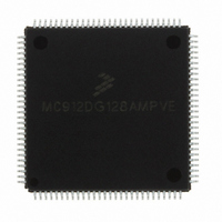
MC912DG128AMPVE Freescale Semiconductor, MC912DG128AMPVE Datasheet - Page 56

MC912DG128AMPVE
Manufacturer Part Number
MC912DG128AMPVE
Description
IC MCU 128K FLASH 8MHZ 112-LQFP
Manufacturer
Freescale Semiconductor
Series
HC12r
Datasheet
1.MC912DG128ACPVER.pdf
(478 pages)
Specifications of MC912DG128AMPVE
Core Processor
CPU12
Core Size
16-Bit
Speed
8MHz
Connectivity
CAN, I²C, SCI, SPI
Peripherals
POR, PWM, WDT
Number Of I /o
69
Program Memory Size
128KB (128K x 8)
Program Memory Type
FLASH
Eeprom Size
2K x 8
Ram Size
8K x 8
Voltage - Supply (vcc/vdd)
4.5 V ~ 5.5 V
Data Converters
A/D 16x8/10b
Oscillator Type
Internal
Operating Temperature
-40°C ~ 125°C
Package / Case
112-LQFP
Processor Series
HC912D
Core
HC12
Data Bus Width
16 bit
Data Ram Size
8 KB
Interface Type
CAN/I2C/SCI/SPI
Maximum Clock Frequency
8 MHz
Number Of Programmable I/os
69
Number Of Timers
8
Maximum Operating Temperature
+ 125 C
Mounting Style
SMD/SMT
3rd Party Development Tools
EWHCS12
Minimum Operating Temperature
- 40 C
On-chip Adc
2 (8-ch x 10-bit)
Lead Free Status / RoHS Status
Lead free / RoHS Compliant
Available stocks
Company
Part Number
Manufacturer
Quantity
Price
Company:
Part Number:
MC912DG128AMPVE
Manufacturer:
FREESCALE
Quantity:
2 902
Company:
Part Number:
MC912DG128AMPVE
Manufacturer:
Freescale Semiconductor
Quantity:
10 000
- Current page: 56 of 478
- Download datasheet (4Mb)
Pinout and Signal Descriptions
3.5 Port Signals
3.5.1 Port A
Technical Data
56
Pin Name
1. MC68HC912DT128A only
KWH[7:0]
KWJ[7:0]
SDA
Shared
PH[7:0]
PJ[7:0]
PIB6
port
Table 3-2. MC68HC912DT128A Signal Description Summary
Number
112-pin
32–35,
19–22
49–52
8–11,
Pin
99
The MC68HC912DT128A incorporates eleven ports which are used to
control and access the various device subsystems. When not used for
these purposes, port pins may be used for general-purpose I/O. In
addition to the pins described below, each port consists of a data register
which can be read and written at any time, and, with the exception of port
AD0, port AD1, PE[1:0], RxCAN and TxCAN, a data direction register
which controls the direction of each pin. After reset all general purpose
I/O pins are configured as input.
Port A pins are used for address and data in expanded modes. When
this port is not used for external access such as in single-chip mode,
these pins can be used as general purpose I/O. The port data register is
not in the address map during expanded and peripheral mode operation.
When it is in the map, port A can be read or written at anytime.
Register DDRA determines whether each port A pin is an input or output.
DDRA is not in the address map during expanded and peripheral mode
operation. Setting a bit in DDRA makes the corresponding bit in port A
an output; clearing a bit in DDRA makes the corresponding bit in port A
an input. The default reset state of DDRA is all zeroes.
When the PUPA bit in the PUCR register is set, all port A input pins are
pulled-up internally by an active pull-up device. PUCR is not in the
address map in peripheral mode.
Freescale Semiconductor, Inc.
For More Information On This Product,
I
Key wake-up and general purpose I/O; can cause an interrupt when an input
Key wake-up and general purpose I/O; can cause an interrupt when an input
2
C bus serial data line pin
transitions from high to low or from low to high (KWPJ).
transitions from high to low or from low to high (KWPH).
Pinout and Signal Descriptions
Go to: www.freescale.com
Description
MC68HC912DT128A — Rev 4.0
MOTOROLA
Related parts for MC912DG128AMPVE
Image
Part Number
Description
Manufacturer
Datasheet
Request
R
Part Number:
Description:
Manufacturer:
Freescale Semiconductor, Inc
Datasheet:
Part Number:
Description:
Manufacturer:
Freescale Semiconductor, Inc
Datasheet:
Part Number:
Description:
Manufacturer:
Freescale Semiconductor, Inc
Datasheet:
Part Number:
Description:
Manufacturer:
Freescale Semiconductor, Inc
Datasheet:
Part Number:
Description:
Manufacturer:
Freescale Semiconductor, Inc
Datasheet:
Part Number:
Description:
Manufacturer:
Freescale Semiconductor, Inc
Datasheet:
Part Number:
Description:
Manufacturer:
Freescale Semiconductor, Inc
Datasheet:
Part Number:
Description:
Manufacturer:
Freescale Semiconductor, Inc
Datasheet:
Part Number:
Description:
Manufacturer:
Freescale Semiconductor, Inc
Datasheet:
Part Number:
Description:
Manufacturer:
Freescale Semiconductor, Inc
Datasheet:
Part Number:
Description:
Manufacturer:
Freescale Semiconductor, Inc
Datasheet:
Part Number:
Description:
Manufacturer:
Freescale Semiconductor, Inc
Datasheet:
Part Number:
Description:
Manufacturer:
Freescale Semiconductor, Inc
Datasheet:
Part Number:
Description:
Manufacturer:
Freescale Semiconductor, Inc
Datasheet:
Part Number:
Description:
Manufacturer:
Freescale Semiconductor, Inc
Datasheet:


