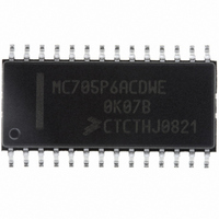
MC705P6ACDWE Freescale Semiconductor, MC705P6ACDWE Datasheet - Page 37

MC705P6ACDWE
Manufacturer Part Number
MC705P6ACDWE
Description
IC MCU 176 BYTES RAM 28-SOIC
Manufacturer
Freescale Semiconductor
Series
HC05r
Datasheet
1.MC705P6ACDWE.pdf
(98 pages)
Specifications of MC705P6ACDWE
Core Processor
HC05
Core Size
8-Bit
Speed
2.1MHz
Connectivity
SIO
Peripherals
POR, WDT
Number Of I /o
21
Program Memory Size
4.5KB (4.5K x 8)
Program Memory Type
OTP
Ram Size
176 x 8
Voltage - Supply (vcc/vdd)
3 V ~ 5.5 V
Data Converters
A/D 4x8b
Oscillator Type
Internal
Operating Temperature
-40°C ~ 85°C
Package / Case
28-SOIC (7.5mm Width)
Processor Series
HC705P
Core
HC05
Data Bus Width
8 bit
Data Ram Size
176 B
Maximum Clock Frequency
2.1 MHz
Number Of Programmable I/os
21
Number Of Timers
1
Maximum Operating Temperature
+ 85 C
Mounting Style
SMD/SMT
Minimum Operating Temperature
- 40 C
On-chip Adc
8 bit, 4 Channel
Lead Free Status / RoHS Status
Lead free / RoHS Compliant
Eeprom Size
-
Lead Free Status / Rohs Status
Details
Available stocks
Company
Part Number
Manufacturer
Quantity
Price
Company:
Part Number:
MC705P6ACDWE
Manufacturer:
Freescale Semiconductor
Quantity:
135
Part Number:
MC705P6ACDWE
Manufacturer:
FREESCALE
Quantity:
20 000
Chapter 6
Input/Output Ports
6.1 Introduction
In the user mode, 20 bidirectional I/O lines are arranged as two 8-bit I/O ports (ports A and C), one 3-bit
I/O port (port B), and one 1-bit I/O port (port D). These ports are programmable as either inputs or outputs
under software control of the data direction registers (DDRs). Port D also contains one input-only pin.
6.2 Port A
Port A is an 8-bit bidirectional port, which does not share any of its pins with other subsystems (see
Figure
located at address $0004. The contents of the port A data register are indeterminate at initial power up
and must be initialized by user software. Reset does not affect the data registers, but does clear the
DDRs, thereby setting all of the port pins to input mode. Writing a 1 to a DDR bit sets the corresponding
port pin to output mode. Port A has mask option register enabled interrupt capability with an internal pullup
device
Freescale Semiconductor
INTERNAL HC05
DATA BUS
6-1). The port A data register is located at address $0000 and its data direction register (DDR) is
WRITE $0004
WRITE $0000
READ $0004
READ $0000
The keyscan (pullup/interrupt) feature available on port A is NOT available
in the ROM device, MC68HC05P6.
RESET
MC68HC705P6A Advance Information Data Sheet, Rev. 2.1
(RST)
Figure 6-1. Port A I/O and Interrupt Circuitry
DATA DIRECTION
REGISTER BIT
REGISTER BIT
DATA
NOTE
OPTION REGISTER
PULLUP MASK
OUTPUT
INTERRUPT SYSTEM
V
TO IRQ
DD
PIN
I/O
37


