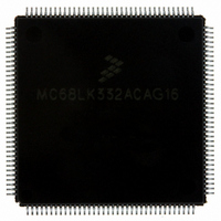
MC68LK332ACAG16 Freescale Semiconductor, MC68LK332ACAG16 Datasheet - Page 27

MC68LK332ACAG16
Manufacturer Part Number
MC68LK332ACAG16
Description
IC MCU 32BIT LV AMASK 144-LQFP
Manufacturer
Freescale Semiconductor
Series
M683xxr
Specifications of MC68LK332ACAG16
Core Processor
CPU32
Core Size
32-Bit
Speed
16.78MHz
Connectivity
EBI/EMI, SCI, SPI, UART/USART
Peripherals
POR, PWM, WDT
Number Of I /o
15
Program Memory Type
ROMless
Ram Size
2K x 8
Voltage - Supply (vcc/vdd)
3 V ~ 3.6 V
Oscillator Type
Internal
Operating Temperature
-40°C ~ 85°C
Package / Case
144-LQFP
Processor Series
M683xx
Core
CPU32
Data Bus Width
32 bit
Maximum Clock Frequency
16 MHz
Maximum Operating Temperature
+ 85 C
Mounting Style
SMD/SMT
Interface Type
QSPI, SCI, UART
Minimum Operating Temperature
- 40 C
No. Of I/o's
15
Ram Memory Size
2KB
Cpu Speed
16MHz
No. Of Timers
16
Embedded Interface Type
QSPI, SCI, UART
Digital Ic Case Style
LQFP
Rohs Compliant
Yes
Data Ram Size
2 KB
Number Of Programmable I/os
15
Number Of Timers
16
Cpu Family
68K/M683xx
Device Core
ColdFire
Device Core Size
32b
Frequency (max)
16MHz
Program Memory Size
Not Required
Total Internal Ram Size
2KB
# I/os (max)
15
Number Of Timers - General Purpose
16
Operating Supply Voltage (typ)
5V
Instruction Set Architecture
RISC
Operating Temp Range
-40C to 85C
Operating Temperature Classification
Industrial
Mounting
Surface Mount
Pin Count
144
Package Type
LQFP
Lead Free Status / RoHS Status
Lead free / RoHS Compliant
Eeprom Size
-
Program Memory Size
-
Data Converters
-
Lead Free Status / Rohs Status
Lead free / RoHS Compliant
Available stocks
Company
Part Number
Manufacturer
Quantity
Price
Company:
Part Number:
MC68LK332ACAG16
Manufacturer:
MOTOLOLA
Quantity:
1 045
Company:
Part Number:
MC68LK332ACAG16
Manufacturer:
Freescale Semiconductor
Quantity:
10 000
Part Number:
MC68LK332ACAG16
Manufacturer:
FREESCALE
Quantity:
20 000
3.4.3 Address Bus
3.4.4 Address Strobe
3.4.5 Data Bus
3.4.6 Data Strobe
3.4.7 Bus Cycle Termination Signals
MC68332
MC68332TS/D
Address bus signals ADDR[23:0] define the address of the most significant byte to be transferred during
a bus cycle. The MCU places the address on the bus at the beginning of a bus cycle. The address is
valid while AS is asserted.
AS is a timing signal that indicates the validity of an address on the address bus and the validity of many
control signals. It is asserted one-half clock after the beginning of a bus cycle.
Data bus signals DATA[15:0] make up a bidirectional, non-multiplexed parallel bus that transfers data
to or from the MCU. A read or write operation can transfer 8 or 16 bits of data in one bus cycle. During
a read cycle, the data is latched by the MCU on the last falling edge of the clock for that bus cycle. For
a write cycle, all 16 bits of the data bus are driven, regardless of the port width or operand size. The
MCU places the data on the data bus one-half clock cycle after AS is asserted in a write cycle.
Data strobe (DS) is a timing signal. For a read cycle, the MCU asserts DS to signal an external device
to place data on the bus. DS is asserted at the same time as AS during a read cycle. For a write cycle,
DS signals an external device that data on the bus is valid. The MCU asserts DS one full clock cycle
after the assertion of AS during a write cycle.
During bus cycles, external devices assert the data transfer and size acknowledge signals (DSACK1
and DSACK0). During a read cycle, the signals tell the MCU to terminate the bus cycle and to latch data.
During a write cycle, the signals indicate that an external device has successfully stored data and that
the cycle can end. These signals also indicate to the MCU the size of the port for the bus cycle just com-
pleted. (Refer to 3.4.9 Dynamic Bus Sizing.)
The bus error (BERR) signal is also a bus cycle termination indicator and can be used in the absence
of DSACK1 and DSACK0 to indicate a bus error condition. It can also be asserted in conjunction with
these signals, provided it meets the appropriate timing requirements. The internal bus monitor can be
used to generate the BERR signal for internal and internal-to-external transfers. When BERR and HALT
are asserted simultaneously, the CPU takes a bus error exception.
Autovector signal (AVEC) can terminate external IRQ pin interrupt acknowledge cycles. AVEC indicates
that the MCU will internally generate a vector number to locate an interrupt handler routine. If it is con-
tinuously asserted, autovectors will be generated for all external interrupt requests. AVEC is ignored
during all other bus cycles.
FC2
0
0
0
0
1
1
1
1
Freescale Semiconductor, Inc.
For More Information On This Product,
Table 9 CPU32 Address Space Encoding
FC1
0
0
1
1
0
0
1
1
Go to: www.freescale.com
FC0
0
1
0
1
0
1
0
1
Supervisor Program Space
Supervisor Data Space
User Program Space
User Data Space
Address Space
CPU Space
Reserved
Reserved
Reserved
MOTOROLA
27


