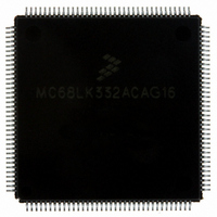
MC68LK332ACAG16 Freescale Semiconductor, MC68LK332ACAG16 Datasheet - Page 37

MC68LK332ACAG16
Manufacturer Part Number
MC68LK332ACAG16
Description
IC MCU 32BIT LV AMASK 144-LQFP
Manufacturer
Freescale Semiconductor
Series
M683xxr
Specifications of MC68LK332ACAG16
Core Processor
CPU32
Core Size
32-Bit
Speed
16.78MHz
Connectivity
EBI/EMI, SCI, SPI, UART/USART
Peripherals
POR, PWM, WDT
Number Of I /o
15
Program Memory Type
ROMless
Ram Size
2K x 8
Voltage - Supply (vcc/vdd)
3 V ~ 3.6 V
Oscillator Type
Internal
Operating Temperature
-40°C ~ 85°C
Package / Case
144-LQFP
Processor Series
M683xx
Core
CPU32
Data Bus Width
32 bit
Maximum Clock Frequency
16 MHz
Maximum Operating Temperature
+ 85 C
Mounting Style
SMD/SMT
Interface Type
QSPI, SCI, UART
Minimum Operating Temperature
- 40 C
No. Of I/o's
15
Ram Memory Size
2KB
Cpu Speed
16MHz
No. Of Timers
16
Embedded Interface Type
QSPI, SCI, UART
Digital Ic Case Style
LQFP
Rohs Compliant
Yes
Data Ram Size
2 KB
Number Of Programmable I/os
15
Number Of Timers
16
Cpu Family
68K/M683xx
Device Core
ColdFire
Device Core Size
32b
Frequency (max)
16MHz
Program Memory Size
Not Required
Total Internal Ram Size
2KB
# I/os (max)
15
Number Of Timers - General Purpose
16
Operating Supply Voltage (typ)
5V
Instruction Set Architecture
RISC
Operating Temp Range
-40C to 85C
Operating Temperature Classification
Industrial
Mounting
Surface Mount
Pin Count
144
Package Type
LQFP
Lead Free Status / RoHS Status
Lead free / RoHS Compliant
Eeprom Size
-
Program Memory Size
-
Data Converters
-
Lead Free Status / Rohs Status
Lead free / RoHS Compliant
Available stocks
Company
Part Number
Manufacturer
Quantity
Price
Company:
Part Number:
MC68LK332ACAG16
Manufacturer:
MOTOLOLA
Quantity:
1 045
Company:
Part Number:
MC68LK332ACAG16
Manufacturer:
Freescale Semiconductor
Quantity:
10 000
Part Number:
MC68LK332ACAG16
Manufacturer:
FREESCALE
Quantity:
20 000
PEPAR — Port E Pin Assignment Register
PORTF0, PORTF1 — Port F Data Register
DDRF — Port F Data Direction Register
MC68332
MC68332TS/D
RESET:
RESET:
RESET:
15
15
15
The bits in this register control the function of each port E pin. Any bit set to one configures the corre-
sponding pin as a bus control signal, with the function shown in the following table. Any bit cleared to
zero defines the corresponding pin to be an I/O pin, controlled by PORTE and DDRE.
Data bus bit 8 controls the state of this register following reset. If DATA8 is set to one during reset, the
register is set to $FF, which defines all port E pins as bus control signals. If DATA8 is cleared to zero
during reset, this register is set to $00, configuring all port E pins as I/O pins.
Any bit cleared to zero defines the corresponding pin to be an I/O pin. Any bit set to one defines the
corresponding pin to be a bus control signal.
The write to the port F data register is stored in the internal data latch, and if any port F pin is configured
as an output, the value stored for that bit is driven onto the pin. A read of the port F data register returns
the value at the pin only if the pin is configured as a discrete input. Otherwise, the value read is the value
stored in the register.
The port F data register is a single register that can be accessed in two locations. When accessed at
$YFFA19, the register is referred to as PORTF0; when accessed at $YFFA1B, the register is referred
to as PORTF1. The register can be read or written at any time. It is unaffected by reset.
The bits in this register control the direction of the pin drivers when the pins are configured for I/O. Any
bit in this register set to one configures the corresponding pin as an output. Any bit in this register
cleared to zero configures the corresponding pin as an input.
PEPAR Bit
PEPA7
PEPA6
PEPA5
PEPA4
PEPA3
PEPA2
PEPA1
PEPA0
NOT USED
NOT USED
NOT USED
Freescale Semiconductor, Inc.
For More Information On This Product,
Table 16 Port E Pin Assignments
Go to: www.freescale.com
Port E Signal
8
PE7
PE6
PE5
PE4
PE3
PE2
PE1
PE0
8
8
PEPA7 PEPA6 PEPA5 PEPA4 PEPA3 PEPA2 PEPA1 PEPA0
DATA8 DATA8 DATA8 DATA8 DATA8 DATA8 DATA8 DATA8
DDF7
PF7
7
7
U
7
0
DDF6
PF6
U
6
6
6
0
DDF5
PF5
U
5
5
5
0
DDF4
PF4
U
4
4
4
0
Bus Control Signal
DDF3
DSACK1
DSACK0
PF3
AVEC
U
3
3
3
0
RMC
SIZ1
SIZ0
AS
DS
$YFFA19, $YFFA1B
DDF2
PF2
U
2
2
2
0
MOTOROLA
DDF1
PF1
$YFFA1D
U
$YFFA17
1
1
1
0
DDF0
PF0
0
0
U
0
0
37


