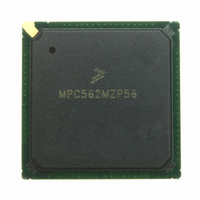
MPC562MZP56 Freescale Semiconductor, MPC562MZP56 Datasheet - Page 1086

MPC562MZP56
Manufacturer Part Number
MPC562MZP56
Description
IC MPU 32BIT 56MHZ PPC 388-PBGA
Manufacturer
Freescale Semiconductor
Series
MPC5xxr
Datasheet
1.MPC561MZP56.pdf
(1420 pages)
Specifications of MPC562MZP56
Core Processor
PowerPC
Core Size
32-Bit
Speed
56MHz
Connectivity
CAN, EBI/EMI, SCI, SPI, UART/USART
Peripherals
POR, PWM, WDT
Number Of I /o
64
Program Memory Type
ROMless
Ram Size
32K x 8
Voltage - Supply (vcc/vdd)
2.5 V ~ 2.7 V
Data Converters
A/D 32x10b
Oscillator Type
External
Operating Temperature
-40°C ~ 125°C
Package / Case
388-BGA
Processor Series
MPC5xx
Core
PowerPC
Data Bus Width
32 bit
Data Ram Size
8 KB
Interface Type
SCI, SPI, UART
Maximum Clock Frequency
40 MHz
Number Of Programmable I/os
56
Number Of Timers
22
Operating Supply Voltage
2.6 V to 5 V
Maximum Operating Temperature
+ 85 C
Mounting Style
SMD/SMT
Minimum Operating Temperature
- 40 C
On-chip Adc
2 (10 bit, 32 Channel)
For Use With
MPC564EVB - KIT EVAL FOR MPC561/562/563/564
Lead Free Status / RoHS Status
Request inventory verification / Request inventory verification
Eeprom Size
-
Program Memory Size
-
Lead Free Status / Rohs Status
No
Available stocks
Company
Part Number
Manufacturer
Quantity
Price
Company:
Part Number:
MPC562MZP56
Manufacturer:
FREESCAL
Quantity:
204
Company:
Part Number:
MPC562MZP56
Manufacturer:
Freescale Semiconductor
Quantity:
10 000
Part Number:
MPC562MZP56
Manufacturer:
FREESCALE
Quantity:
20 000
Company:
Part Number:
MPC562MZP56R2
Manufacturer:
RFT
Quantity:
1 441
Company:
Part Number:
MPC562MZP56R2
Manufacturer:
Freescale Semiconductor
Quantity:
10 000
- Current page: 1086 of 1420
- Download datasheet (11Mb)
IEEE 1149.1-Compliant Interface (JTAG)
25.1.3.4
The CLAMP instruction selects the single-bit bypass register as shown in
signals driven from system output pins is completely defined by the data previously shifted into the
boundary scan register (for example, using the SAMPLE/PRELOAD instruction).
25.1.4
The HI-Z instruction is provided as a manufacturer’s optional public instruction to prevent having to
backdrive the output pins during circuit-board testing. When HI-Z is invoked, all output drivers, including
the two-state drivers, are turned off (i.e., high impedance). The instruction selects the bypass register.
25.2
The control afforded by the output enable signals using the boundary scan register and the EXTEST
instruction requires a compatible circuit-board test environment to avoid device-destructive
configurations. The user must avoid situations in which the MPC561/MPC563 output drivers are enabled
into actively driven networks.
The MPC561/MPC563 features a low-power stop mode. The interaction of the scan chain interface with
low-power stop mode is as follows:
25.2.1
In non-scan chain operation, there are two constraints. First, the TCK input does not include an internal
pull-up resistor and should not be left unconnected to preclude mid-level inputs. The second constraint is
to ensure that the scan chain test logic is kept transparent to the system logic by forcing TAP into the
test-logic-reset controller state, using either of two methods. Connecting pin JCOMP to logic 0 (or one of
the reset pins), or TMS must be sampled as a logic one for five consecutive TCK rising edges. If then TMS
either remains unconnected or is connected to V
test-logic-reset state, regardless of the state of TCK.
25-32
1. The TAP controller must be in the test-logic-reset state to either enter or remain in the low-power
2. The TCK input is not blocked in low-power stop mode. To consume minimal power, the TCK input
3. The TMS pin includes an on-chip pull-up resistor. In low-power stop mode, this pin should remain
4. JCOMP must be low prior to PORESET assertion after low power mode exits otherwise an
stop mode. Leaving the TAP controller in the test-logic-reset state negates the ability to achieve
low-power, but does not otherwise affect device functionality.
should be externally connected to V
either unconnected or connected to VDD to achieve minimal power consumption. Note that for
proper reset of the scan chain test logic, the best approach is to pull JCOMP low at power-on reset
(PORESET).
unknown state will occur.
MPC561/MPC563 Restrictions
HI-Z
Non-Scan Chain Operation
CLAMP
MPC561/MPC563 Reference Manual, Rev. 1.2
DD
or ground.
DD
, then the TAP controller cannot leave the
Figure
25-5, and the state of all
Freescale Semiconductor
Related parts for MPC562MZP56
Image
Part Number
Description
Manufacturer
Datasheet
Request
R
Part Number:
Description:
Mpc562 32 Bit Powerpc Microcontroller
Manufacturer:
Freescale Semiconductor, Inc
Datasheet:

Part Number:
Description:
MPC5 1K0 5%
Manufacturer:
TE Connectivity
Datasheet:

Part Number:
Description:
MPC5 500R 5%
Manufacturer:
TE Connectivity
Datasheet:

Part Number:
Description:
MPC5 5K0 5%
Manufacturer:
Tyco Electronics
Datasheet:

Part Number:
Description:
MPC5 5R0 5%
Manufacturer:
Tyco Electronics
Datasheet:

Part Number:
Description:
MPC5 50K 5%
Manufacturer:
Tyco Electronics
Datasheet:
Part Number:
Description:
Manufacturer:
Freescale Semiconductor, Inc
Datasheet:
Part Number:
Description:
Manufacturer:
Freescale Semiconductor, Inc
Datasheet:
Part Number:
Description:
Manufacturer:
Freescale Semiconductor, Inc
Datasheet:
Part Number:
Description:
Manufacturer:
Freescale Semiconductor, Inc
Datasheet:
Part Number:
Description:
Manufacturer:
Freescale Semiconductor, Inc
Datasheet:


