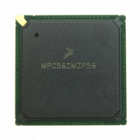
MPC562MZP56 Freescale Semiconductor, MPC562MZP56 Datasheet - Page 402

MPC562MZP56
Manufacturer Part Number
MPC562MZP56
Description
IC MPU 32BIT 56MHZ PPC 388-PBGA
Manufacturer
Freescale Semiconductor
Series
MPC5xxr
Datasheet
1.MPC561MZP56.pdf
(1420 pages)
Specifications of MPC562MZP56
Core Processor
PowerPC
Core Size
32-Bit
Speed
56MHz
Connectivity
CAN, EBI/EMI, SCI, SPI, UART/USART
Peripherals
POR, PWM, WDT
Number Of I /o
64
Program Memory Type
ROMless
Ram Size
32K x 8
Voltage - Supply (vcc/vdd)
2.5 V ~ 2.7 V
Data Converters
A/D 32x10b
Oscillator Type
External
Operating Temperature
-40°C ~ 125°C
Package / Case
388-BGA
Processor Series
MPC5xx
Core
PowerPC
Data Bus Width
32 bit
Data Ram Size
8 KB
Interface Type
SCI, SPI, UART
Maximum Clock Frequency
40 MHz
Number Of Programmable I/os
56
Number Of Timers
22
Operating Supply Voltage
2.6 V to 5 V
Maximum Operating Temperature
+ 85 C
Mounting Style
SMD/SMT
Minimum Operating Temperature
- 40 C
On-chip Adc
2 (10 bit, 32 Channel)
For Use With
MPC564EVB - KIT EVAL FOR MPC561/562/563/564
Lead Free Status / RoHS Status
Request inventory verification / Request inventory verification
Eeprom Size
-
Program Memory Size
-
Lead Free Status / Rohs Status
No
Available stocks
Company
Part Number
Manufacturer
Quantity
Price
Company:
Part Number:
MPC562MZP56
Manufacturer:
FREESCAL
Quantity:
204
Company:
Part Number:
MPC562MZP56
Manufacturer:
Freescale Semiconductor
Quantity:
10 000
Part Number:
MPC562MZP56
Manufacturer:
FREESCALE
Quantity:
20 000
Company:
Part Number:
MPC562MZP56R2
Manufacturer:
RFT
Quantity:
1 441
Company:
Part Number:
MPC562MZP56R2
Manufacturer:
Freescale Semiconductor
Quantity:
10 000
- Current page: 402 of 1420
- Download datasheet (11Mb)
Memory Controller
When a match is found on one of the memory banks, its attributes are selected for the functional operation
of the external memory access:
Note that if more than one region matches the internal address supplied, then the lowest numbered region
is selected to provide the attributes and the chip select. If the dual mapping region is matched, it has the
highest priority (refer to
10.2.1
Status bits for each memory bank are found in the memory control status register (MSTAT). The MSTAT
reports write-protect violations for all the banks.
Each of the four memory banks has a base register (BR) and an option register (OR). The BRx and ORx
registers contain the attributes specific to memory bank x. The base register contains a valid bit (V) that
indicates the register information for that particular chip select is valid.
10.2.2
The memory controller supports dynamic bus sizing. Defined 8-bit ports can be accessed as odd or even
bytes. Defined 16-bit ports, when connected to data bus lines zero to 15, can be accessed as odd bytes, even
bytes, or even half-words. Defined 32-bit ports can be accessed as odd bytes, even bytes, odd half-words,
even half-words, or words on word boundaries. The port size is specified by the PS bits in the base register.
10-4
•
•
•
•
A[0:16]
Read-only or read/write operations
Number of wait states for a single memory access, and for any beat in a burst access
Burst-inhibit indication. Internal burst requests are still possible during burst-inhibited cycles; the
memory controller emulates the burst cycles
Port size of the external device
cmp cmp cmp cmp cmpcmpcmp
Associated Registers
Port Size Configuration
Base Address
Section 10.5, “Dual Mapping of the Internal Flash EEPROM
Figure 10-4. Bank Base Address and Match Structure
. . . . . . . . . . . . .
MPC561/MPC563 Reference Manual, Rev. 1.2
cmp
cmp cmp cmp
M0 M1 M2 M3 M4 M5
M[0:16]
Address Mask
Match
M6 M7
Freescale Semiconductor
Array”).
. . . .
M16
Related parts for MPC562MZP56
Image
Part Number
Description
Manufacturer
Datasheet
Request
R
Part Number:
Description:
Mpc562 32 Bit Powerpc Microcontroller
Manufacturer:
Freescale Semiconductor, Inc
Datasheet:

Part Number:
Description:
MPC5 1K0 5%
Manufacturer:
TE Connectivity
Datasheet:

Part Number:
Description:
MPC5 500R 5%
Manufacturer:
TE Connectivity
Datasheet:

Part Number:
Description:
MPC5 5K0 5%
Manufacturer:
Tyco Electronics
Datasheet:

Part Number:
Description:
MPC5 5R0 5%
Manufacturer:
Tyco Electronics
Datasheet:

Part Number:
Description:
MPC5 50K 5%
Manufacturer:
Tyco Electronics
Datasheet:
Part Number:
Description:
Manufacturer:
Freescale Semiconductor, Inc
Datasheet:
Part Number:
Description:
Manufacturer:
Freescale Semiconductor, Inc
Datasheet:
Part Number:
Description:
Manufacturer:
Freescale Semiconductor, Inc
Datasheet:
Part Number:
Description:
Manufacturer:
Freescale Semiconductor, Inc
Datasheet:
Part Number:
Description:
Manufacturer:
Freescale Semiconductor, Inc
Datasheet:


