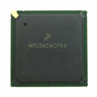
MPC562MZP56 Freescale Semiconductor, MPC562MZP56 Datasheet - Page 556

MPC562MZP56
Manufacturer Part Number
MPC562MZP56
Description
IC MPU 32BIT 56MHZ PPC 388-PBGA
Manufacturer
Freescale Semiconductor
Series
MPC5xxr
Datasheet
1.MPC561MZP56.pdf
(1420 pages)
Specifications of MPC562MZP56
Core Processor
PowerPC
Core Size
32-Bit
Speed
56MHz
Connectivity
CAN, EBI/EMI, SCI, SPI, UART/USART
Peripherals
POR, PWM, WDT
Number Of I /o
64
Program Memory Type
ROMless
Ram Size
32K x 8
Voltage - Supply (vcc/vdd)
2.5 V ~ 2.7 V
Data Converters
A/D 32x10b
Oscillator Type
External
Operating Temperature
-40°C ~ 125°C
Package / Case
388-BGA
Processor Series
MPC5xx
Core
PowerPC
Data Bus Width
32 bit
Data Ram Size
8 KB
Interface Type
SCI, SPI, UART
Maximum Clock Frequency
40 MHz
Number Of Programmable I/os
56
Number Of Timers
22
Operating Supply Voltage
2.6 V to 5 V
Maximum Operating Temperature
+ 85 C
Mounting Style
SMD/SMT
Minimum Operating Temperature
- 40 C
On-chip Adc
2 (10 bit, 32 Channel)
For Use With
MPC564EVB - KIT EVAL FOR MPC561/562/563/564
Lead Free Status / RoHS Status
Request inventory verification / Request inventory verification
Eeprom Size
-
Program Memory Size
-
Lead Free Status / Rohs Status
No
Available stocks
Company
Part Number
Manufacturer
Quantity
Price
Company:
Part Number:
MPC562MZP56
Manufacturer:
FREESCAL
Quantity:
204
Company:
Part Number:
MPC562MZP56
Manufacturer:
Freescale Semiconductor
Quantity:
10 000
Part Number:
MPC562MZP56
Manufacturer:
FREESCALE
Quantity:
20 000
Company:
Part Number:
MPC562MZP56R2
Manufacturer:
RFT
Quantity:
1 441
Company:
Part Number:
MPC562MZP56R2
Manufacturer:
Freescale Semiconductor
Quantity:
10 000
- Current page: 556 of 1420
- Download datasheet (11Mb)
QADC64E Enhanced Mode Operation
configures the corresponding signal as an input. The software is responsible for ensuring that DDR bits are
not set to one on signals used for analog inputs. When the DDR bit is set to one and the signal is selected
for analog conversion, the voltage sampled is that of the output digital driver as influenced by the load.
There are two special cases to consider for the digital I/O port operation. When QACR0[EMUX] bit is set,
enabling external multiplexing, the data direction register settings are ignored for the bits corresponding
to PORTQA[2:0], which are the three multiplexed address output signals, MA[2:0]. The MA[2:0] signals
are forced to be digital outputs, regardless of the data direction setting, and the multiplexed address outputs
are driven. The data returned during a port data register read is the value of the multiplexed address latches
which drive MA[2:0], regardless of the data direction setting.
14.3.5
Control Register 0 defines whether external multiplexing is enabled, assigns external triggers to the
conversion queues and sets up the QCLK prescaler parameter field. All of the implemented control register
fields can be read or written but reserved fields read zero and writes have no effect. Typically, they are
written once when software initializes the QADC64E and are not changed afterwards.
14-14
SRESET
Field
SRESET
Addr
Field DDQ
Addr
EMUX
Control Register 0
MSB
0
0
MSB
A7
Caution should be exercised when mixing digital and analog inputs. This
should be isolated as much as possible. Rise and fall times should be as large
as possible to minimize AC coupling effects.
0
0x30 4808 (DDRQA_A); 0x30 4C08 (DDRQA_B); 0x30 4809 (DDRQB_A); 0x30 4C09 (DDRQB_B)
DDQ
1
0
A6
Figure 14-8. Portx Data Direction Register (DDRQA and DDRQB)
1
—
DDQ
0
2
A5
2
TRG
DDQ
3
0
A4
Figure 14-9. Control Register 0 (QACR0)
MPC561/MPC563 Reference Manual, Rev. 1.2
3
0x30 480A (QACR0_A); 0x30 4C0A (QACR0_B)
DDQ
0
4
A3
4
0
DDQ
5
A2
5
0000_0000_0000_0000
—
0
6
NOTE
DDQ
A1
6
0
7
DDQ
A0
7
0
8
DDQ
B7
8
0
9
DDQ
B6
9
DDQ
10
0
B5
10
DDQ
11
B4
1
11
PRESCALER
DDQ
B3
12
12
0
Freescale Semiconductor
DDQ
B2
13
13
0
DDQ
B1
14
14
1
DDQ
LSB
B0
15
LSB
15
1
Related parts for MPC562MZP56
Image
Part Number
Description
Manufacturer
Datasheet
Request
R
Part Number:
Description:
Mpc562 32 Bit Powerpc Microcontroller
Manufacturer:
Freescale Semiconductor, Inc
Datasheet:

Part Number:
Description:
MPC5 1K0 5%
Manufacturer:
TE Connectivity
Datasheet:

Part Number:
Description:
MPC5 500R 5%
Manufacturer:
TE Connectivity
Datasheet:

Part Number:
Description:
MPC5 5K0 5%
Manufacturer:
Tyco Electronics
Datasheet:

Part Number:
Description:
MPC5 5R0 5%
Manufacturer:
Tyco Electronics
Datasheet:

Part Number:
Description:
MPC5 50K 5%
Manufacturer:
Tyco Electronics
Datasheet:
Part Number:
Description:
Manufacturer:
Freescale Semiconductor, Inc
Datasheet:
Part Number:
Description:
Manufacturer:
Freescale Semiconductor, Inc
Datasheet:
Part Number:
Description:
Manufacturer:
Freescale Semiconductor, Inc
Datasheet:
Part Number:
Description:
Manufacturer:
Freescale Semiconductor, Inc
Datasheet:
Part Number:
Description:
Manufacturer:
Freescale Semiconductor, Inc
Datasheet:


