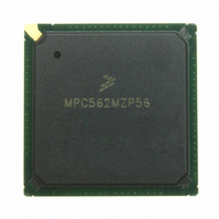
MPC562MZP56 Freescale Semiconductor, MPC562MZP56 Datasheet - Page 628

MPC562MZP56
Manufacturer Part Number
MPC562MZP56
Description
IC MPU 32BIT 56MHZ PPC 388-PBGA
Manufacturer
Freescale Semiconductor
Series
MPC5xxr
Datasheet
1.MPC561MZP56.pdf
(1420 pages)
Specifications of MPC562MZP56
Core Processor
PowerPC
Core Size
32-Bit
Speed
56MHz
Connectivity
CAN, EBI/EMI, SCI, SPI, UART/USART
Peripherals
POR, PWM, WDT
Number Of I /o
64
Program Memory Type
ROMless
Ram Size
32K x 8
Voltage - Supply (vcc/vdd)
2.5 V ~ 2.7 V
Data Converters
A/D 32x10b
Oscillator Type
External
Operating Temperature
-40°C ~ 125°C
Package / Case
388-BGA
Processor Series
MPC5xx
Core
PowerPC
Data Bus Width
32 bit
Data Ram Size
8 KB
Interface Type
SCI, SPI, UART
Maximum Clock Frequency
40 MHz
Number Of Programmable I/os
56
Number Of Timers
22
Operating Supply Voltage
2.6 V to 5 V
Maximum Operating Temperature
+ 85 C
Mounting Style
SMD/SMT
Minimum Operating Temperature
- 40 C
On-chip Adc
2 (10 bit, 32 Channel)
For Use With
MPC564EVB - KIT EVAL FOR MPC561/562/563/564
Lead Free Status / RoHS Status
Request inventory verification / Request inventory verification
Eeprom Size
-
Program Memory Size
-
Lead Free Status / Rohs Status
No
Available stocks
Company
Part Number
Manufacturer
Quantity
Price
Company:
Part Number:
MPC562MZP56
Manufacturer:
FREESCAL
Quantity:
204
Company:
Part Number:
MPC562MZP56
Manufacturer:
Freescale Semiconductor
Quantity:
10 000
Part Number:
MPC562MZP56
Manufacturer:
FREESCALE
Quantity:
20 000
Company:
Part Number:
MPC562MZP56R2
Manufacturer:
RFT
Quantity:
1 441
Company:
Part Number:
MPC562MZP56R2
Manufacturer:
Freescale Semiconductor
Quantity:
10 000
- Current page: 628 of 1420
- Download datasheet (11Mb)
Queued Serial Multi-Channel Module
15.5
Table 15-7
The QSMCM uses 11 pins. These pins, when not being used by the serial sub-systems, form a parallel port
on the MCU.
The port QS pin assignment register (PQSPAR) governs the usage of QSPI pins. Clearing a bit assigns the
corresponding pin to general-purpose I/O; setting a bit assigns the pin to the QSPI.
PQSPAR does not affect operation of the SCI. When the SCIx transmitter is disabled, TXDx is a discrete
output; when the SCIx receiver is disabled, RXDx is a discrete input. When the SCIx transmitter or
receiver is enabled, the associated TXDx or RXDx pin is assigned its SCI function.
The port QS data direction register (DDRQS) determines whether QSPI pins are inputs or outputs.
Clearing a bit makes the corresponding pin an input; setting a bit makes the pin an output. DDRQS affects
both QSPI function and I/O function.
function.
DDRQS does not affect SCI pin function. TXDx pins are always outputs, and RXDx pins are always
inputs, regardless of whether they are functioning as SCI pins or as PORTQS pins.
15-10
SRESET
11:15
Bits
0:10
Field
Addr
QSMCM Pin Control Registers
lists the three QSMCM pin control registers.
MSB
0x30 5014
0x30 5016
0x30 5017
Address
0
ILQSPI
Name
—
1
Figure 15-6. QSPI_IL — QSPI Interrupt Level Register
2
QSMCM Port Data Register (PORTQS)
See Section 15.5.1, “Port QS Data Register (PORTQS) for bit descriptions.
PORTQS Pin Assignment Register (PQSPAR)
See <XrefBlue>Table 15-10 for bit descriptions.
PORTQS Data Direction Register (DDRQS)
See <XrefBlue>Table 15-10 for bit descriptions.
Reserved
Interrupt level of SPI
00000lowest interrupt level request (level 0)
11111highest interrupt level request (level 31)
Table 15-7. QSMCM Pin Control Registers
MPC561/MPC563 Reference Manual, Rev. 1.2
3
Table 15-6. QSPI_IL Bit Descriptions
Table 15-8
4
—
5
0000_0000_0000_0000
6
summarizes the effect of DDRQS bits on QSPI pin
0x30 5006
7
Register
Description
8
9
10
11
12
Freescale Semiconductor
ILQSPI
13
14
LSB
15
Related parts for MPC562MZP56
Image
Part Number
Description
Manufacturer
Datasheet
Request
R
Part Number:
Description:
Mpc562 32 Bit Powerpc Microcontroller
Manufacturer:
Freescale Semiconductor, Inc
Datasheet:

Part Number:
Description:
MPC5 1K0 5%
Manufacturer:
TE Connectivity
Datasheet:

Part Number:
Description:
MPC5 500R 5%
Manufacturer:
TE Connectivity
Datasheet:

Part Number:
Description:
MPC5 5K0 5%
Manufacturer:
Tyco Electronics
Datasheet:

Part Number:
Description:
MPC5 5R0 5%
Manufacturer:
Tyco Electronics
Datasheet:

Part Number:
Description:
MPC5 50K 5%
Manufacturer:
Tyco Electronics
Datasheet:
Part Number:
Description:
Manufacturer:
Freescale Semiconductor, Inc
Datasheet:
Part Number:
Description:
Manufacturer:
Freescale Semiconductor, Inc
Datasheet:
Part Number:
Description:
Manufacturer:
Freescale Semiconductor, Inc
Datasheet:
Part Number:
Description:
Manufacturer:
Freescale Semiconductor, Inc
Datasheet:
Part Number:
Description:
Manufacturer:
Freescale Semiconductor, Inc
Datasheet:


