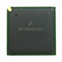
MPC562MZP56 Freescale Semiconductor, MPC562MZP56 Datasheet - Page 876

MPC562MZP56
Manufacturer Part Number
MPC562MZP56
Description
IC MPU 32BIT 56MHZ PPC 388-PBGA
Manufacturer
Freescale Semiconductor
Series
MPC5xxr
Datasheet
1.MPC561MZP56.pdf
(1420 pages)
Specifications of MPC562MZP56
Core Processor
PowerPC
Core Size
32-Bit
Speed
56MHz
Connectivity
CAN, EBI/EMI, SCI, SPI, UART/USART
Peripherals
POR, PWM, WDT
Number Of I /o
64
Program Memory Type
ROMless
Ram Size
32K x 8
Voltage - Supply (vcc/vdd)
2.5 V ~ 2.7 V
Data Converters
A/D 32x10b
Oscillator Type
External
Operating Temperature
-40°C ~ 125°C
Package / Case
388-BGA
Processor Series
MPC5xx
Core
PowerPC
Data Bus Width
32 bit
Data Ram Size
8 KB
Interface Type
SCI, SPI, UART
Maximum Clock Frequency
40 MHz
Number Of Programmable I/os
56
Number Of Timers
22
Operating Supply Voltage
2.6 V to 5 V
Maximum Operating Temperature
+ 85 C
Mounting Style
SMD/SMT
Minimum Operating Temperature
- 40 C
On-chip Adc
2 (10 bit, 32 Channel)
For Use With
MPC564EVB - KIT EVAL FOR MPC561/562/563/564
Lead Free Status / RoHS Status
Request inventory verification / Request inventory verification
Eeprom Size
-
Program Memory Size
-
Lead Free Status / Rohs Status
No
Available stocks
Company
Part Number
Manufacturer
Quantity
Price
Company:
Part Number:
MPC562MZP56
Manufacturer:
FREESCAL
Quantity:
204
Company:
Part Number:
MPC562MZP56
Manufacturer:
Freescale Semiconductor
Quantity:
10 000
Part Number:
MPC562MZP56
Manufacturer:
FREESCALE
Quantity:
20 000
Company:
Part Number:
MPC562MZP56R2
Manufacturer:
RFT
Quantity:
1 441
Company:
Part Number:
MPC562MZP56R2
Manufacturer:
Freescale Semiconductor
Quantity:
10 000
- Current page: 876 of 1420
- Download datasheet (11Mb)
CDR3 Flash (UC3F) EEPROM
21-14
Bits
30
31
PEGOOD
Name
SES
EHV
EHV
HVS
SES
Start-end program or erase sequence. The SES bit is write protected by the STOP, HVS, and
EHV bits. The SES bit is used to signal the start and end of a program or erase sequence. At
the start of a program or erase sequence, SES is set. This will lock STOP, PROTECT,
SBPROTECT, BLOCK, SBBLOCK, SBEN, CSC, and PE. If PE = 0 and SES = 1, SIE will be write
locked. At this point, the UC3F EEPROM is ready to receive either the programming writes or
the erase interlock write.
NOTE: The erase interlock write is a write to any UC3F EEPROM array location after SES is set
and PE = 1.
If PE = 0 and SES = 1, writes to the UC3F array are programming writes. The first programming
write sets the address of the location to be programmed, and the data written is captured into
the program data latch for programming into the UC3F array. All programming writes after the
first programming write update the program data latch but do not change the address to be
programmed.
At the end of the program or erase operation, the SES bit must be cleared to return to normal
operation and release the STOP, PROTECT, SBPROTECT, BLOCK, SBBLOCK, CSC, SBEN,
and PE bits.
0 UC3F EEPROM not configured for program or erase operation
1 Configure UC3F EEPROM for program or erase operation
Enable high voltage. EHV can be asserted only after the SES bit has been asserted and a valid
programming write(s) or erase hardware interlock write has occurred. If an attempt is made to
assert EHV when SES is negated, or if a valid programming write or erase hardware interlock
write has not occurred since SES was asserted, EHV will remain negated.
The external program or erase enable pin (EPEE) and EHV are used to control the application
of the program or erase voltage to the UC3F EEPROM module. High voltage operations to the
UC3F EEPROM array, special shadow locations or FLASH NVM registers can occur only if
EHV = 1 and EPEE = 1.
Only after the correct hardware and software interlocks have been applied to the UC3F
EEPROM can EHV be set. Once EHV is set, SES cannot be changed and attempts to read the
array will not be acknowledged.
Clearing EHV during a program or erase operation will safely terminate the high voltage
operation. If EHV is cleared while using the embedded hardware program/erase algorithm, the
program/erase routine will abort the operation and exit normally.
0 Program or erase pulse disabled
1 Program or erase pulse enabled
Table 21-5. UC3FCTL Bit Descriptions (continued)
MPC561/MPC563 Reference Manual, Rev. 1.2
Figure 21-5. PEGOOD Valid Time
Valid Time
PEGOOD
Description
Valid Time
PEGOOD
Freescale Semiconductor
Related parts for MPC562MZP56
Image
Part Number
Description
Manufacturer
Datasheet
Request
R
Part Number:
Description:
Mpc562 32 Bit Powerpc Microcontroller
Manufacturer:
Freescale Semiconductor, Inc
Datasheet:

Part Number:
Description:
MPC5 1K0 5%
Manufacturer:
TE Connectivity
Datasheet:

Part Number:
Description:
MPC5 500R 5%
Manufacturer:
TE Connectivity
Datasheet:

Part Number:
Description:
MPC5 5K0 5%
Manufacturer:
Tyco Electronics
Datasheet:

Part Number:
Description:
MPC5 5R0 5%
Manufacturer:
Tyco Electronics
Datasheet:

Part Number:
Description:
MPC5 50K 5%
Manufacturer:
Tyco Electronics
Datasheet:
Part Number:
Description:
Manufacturer:
Freescale Semiconductor, Inc
Datasheet:
Part Number:
Description:
Manufacturer:
Freescale Semiconductor, Inc
Datasheet:
Part Number:
Description:
Manufacturer:
Freescale Semiconductor, Inc
Datasheet:
Part Number:
Description:
Manufacturer:
Freescale Semiconductor, Inc
Datasheet:
Part Number:
Description:
Manufacturer:
Freescale Semiconductor, Inc
Datasheet:


