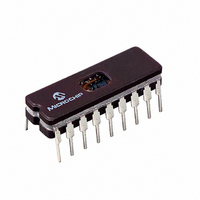
PIC16C56A/JW Microchip Technology, PIC16C56A/JW Datasheet - Page 38

PIC16C56A/JW
Manufacturer Part Number
PIC16C56A/JW
Description
IC MCU EPROM 1KX12 18CDIP
Manufacturer
Microchip Technology
Series
PIC® 16Cr
Specifications of PIC16C56A/JW
Core Processor
PIC
Core Size
8-Bit
Speed
20MHz
Peripherals
POR, WDT
Number Of I /o
12
Program Memory Size
1.5KB (1K x 12)
Program Memory Type
EPROM, UV
Ram Size
25 x 8
Voltage - Supply (vcc/vdd)
3 V ~ 5.5 V
Oscillator Type
External
Operating Temperature
0°C ~ 70°C
Package / Case
18-CDIP (0.300", 7.62mm) Window
Lead Free Status / RoHS Status
Contains lead / RoHS non-compliant
Eeprom Size
-
Data Converters
-
Connectivity
-
Available stocks
Company
Part Number
Manufacturer
Quantity
Price
Company:
Part Number:
PIC16C56A/JW
Manufacturer:
Microchip Technology
Quantity:
2
- Current page: 38 of 194
- Download datasheet (3Mb)
PIC16C5X
7.6
7.6.1
Some instructions operate internally as read followed
by write operations. The BCF and BSF instructions, for
example, read the entire port into the CPU, execute the
bit operation and re-write the result. Caution must be
used when these instructions are applied to a port
where one or more pins are used as input/outputs. For
example, a BSF operation on bit5 of PORTB will cause
all eight bits of PORTB to be read into the CPU, bit5 to
be set and the PORTB value to be written to the output
latches. If another bit of PORTB is used as a bi-direc-
tional I/O pin (say bit0) and it is defined as an input at
this time, the input signal present on the pin itself would
be read into the CPU and rewritten to the data latch of
this particular pin, overwriting the previous content. As
long as the pin stays in the Input mode, no problem
occurs. However, if bit0 is switched into Output mode
later on, the content of the data latch may now be
unknown.
Example 7-1 shows the effect of two sequential read-
modify-write instructions (e.g., BCF, BSF, etc.) on an
I/O port.
A pin actively outputting a high or a low should not be
driven from external devices at the same time in order
to change the level on this pin (“wired-or”, “wired-and”).
The resulting high output currents may damage the
chip.
FIGURE 7-2:
DS30453D-page 36
Instruction
Instruction
I/O Programming Considerations
executed
RB<7:0>
fetched
BI-DIRECTIONAL I/O PORTS
Q1 Q2 Q3 Q4 Q1 Q2 Q3 Q4 Q1 Q2 Q3 Q4 Q1 Q2 Q3 Q4
MOVWF PORTB
SUCCESSIVE I/O OPERATION
PC
MOVF PORTB,W
MOVWF PORTB
(Write to
PORTB)
written here
PC + 1
Port pin
MOVF PORTB,W
Preliminary
(Read
sampled here
PORTB)
NOP
PC + 2
Port pin
EXAMPLE 7-1:
;Initial PORT Settings
; PORTB<7:4> Inputs
; PORTB<3:0> Outputs
;PORTB<7:6> have external pull-ups and are
;not connected to other circuitry
;
;
;
;
;Note that the user may have expected the pin
;values to be 00pp pppp. The 2nd BCF caused
;RB7 to be latched as the pin value (High).
7.6.2
The actual write to an I/O port happens at the end of an
instruction cycle, whereas for reading, the data must be
valid at the beginning of the instruction cycle (Figure 7-
2). Therefore, care must be exercised if a write followed
by a read operation is carried out on the same I/O port.
The sequence of instructions should allow the pin volt-
age to stabilize (load dependent) before the next
instruction, which causes that file to be read into the
CPU, is executed. Otherwise, the previous state of that
pin may be read into the CPU rather than the new state.
When in doubt, it is better to separate these instruc-
tions with a NOP or another instruction not accessing
this I/O port.
BCF
BCF
MOVLW H’3F’
TRIS
PC + 3
NOP
NOP
PORTB, 7
PORTB, 6
PORTB
SUCCESSIVE OPERATIONS ON I/O
PORTS
This example shows a write
to PORTB followed by a read
from PORTB.
INSTRUCTIONS ON AN I/O
PORT
READ-MODIFY-WRITE
;01pp pppp
;10pp pppp
;10pp pppp
PORT latch
;
----------
2002 Microchip Technology Inc.
PORT pins
----------
11pp pppp
11pp pppp
10pp pppp
Related parts for PIC16C56A/JW
Image
Part Number
Description
Manufacturer
Datasheet
Request
R

Part Number:
Description:
Manufacturer:
Microchip Technology Inc.
Datasheet:

Part Number:
Description:
IC MCU OTP 1KX12 18SOIC
Manufacturer:
Microchip Technology
Datasheet:

Part Number:
Description:
IC MCU OTP 1KX12 18DIP
Manufacturer:
Microchip Technology
Datasheet:

Part Number:
Description:
IC MCU OTP 1KX12 18DIP
Manufacturer:
Microchip Technology
Datasheet:

Part Number:
Description:
IC MCU OTP 1KX12 18DIP
Manufacturer:
Microchip Technology
Datasheet:

Part Number:
Description:
IC MCU OTP 1KX12 18DIP
Manufacturer:
Microchip Technology
Datasheet:

Part Number:
Description:
IC MCU OTP 1KX12 18SOIC
Manufacturer:
Microchip Technology
Datasheet:

Part Number:
Description:
IC MCU OTP 1KX12 18DIP
Manufacturer:
Microchip Technology
Datasheet:

Part Number:
Description:
IC MCU OTP 1KX12 18SOIC
Manufacturer:
Microchip Technology
Datasheet:

Part Number:
Description:
IC MCU OTP 1KX12 20SSOP
Manufacturer:
Microchip Technology
Datasheet:

Part Number:
Description:
IC MCU OTP 1KX12 20SSOP
Manufacturer:
Microchip Technology
Datasheet:

Part Number:
Description:
IC MCU OTP 1KX12 18SOIC
Manufacturer:
Microchip Technology
Datasheet:

Part Number:
Description:
IC MCU OTP 1KX12 18DIP
Manufacturer:
Microchip Technology
Datasheet:

Part Number:
Description:
IC MCU OTP 1KX12 18DIP
Manufacturer:
Microchip Technology
Datasheet:

Part Number:
Description:
IC MCU OTP 1KX12 18DIP
Manufacturer:
Microchip Technology
Datasheet:


