KT3225F16369ACW28TA0 AVX Corporation, KT3225F16369ACW28TA0 Datasheet - Page 4
KT3225F16369ACW28TA0
Manufacturer Part Number
KT3225F16369ACW28TA0
Description
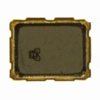
OSCILLATOR TCXO 16.369MHZ SMD
Manufacturer
AVX Corporation
Series
KT3225F, Kyocerar
Type
TCXOr
Specifications of KT3225F16369ACW28TA0
Package / Case
SMD 3.20mm x 2.50mm
Frequency
16.369MHz
Supply Voltage
2.8V
Frequency Stability
±0.5ppm
Operating Temperature
-30°C ~ 85°C
Current - Supply (max)
2mA
Mounting Type
Surface Mount
Size / Dimension
0.126" L x 0.098" W (3.20mm x 2.50mm)
Height
0.039" (1.00mm)
Supply Current
2mA
Termination Style
SMD/SMT
Dimensions
2.5 mm W x 3.2 mm L x 1 mm H
Mounting Style
SMD/SMT
Product
TCXO
Lead Free Status / RoHS Status
Lead free / RoHS Compliant
Lead Free Status / RoHS Status
Lead free / RoHS Compliant, Lead free / RoHS Compliant
Other names
478-4826-2
KT3225F16369ACW28TB0
KT3225F16369ACW28TB0


Specifications
Dimensions
Output Frequency
Frequency Tolerance
Frequency Aging
Storage Temperature Range
Operating Temperature Range
Voltage Control Range
Supply Voltage
Output Level
Current Consumption
Symmetry
Harmonics
Pb Free
KT5032N
0.925
#1
#4
Item
KSS001
5.00.15
Temperature Compensated Crystal Oscillators (TCXO)
Surface Mount Type TCXO (LSI Type) KT5032 Series
5.0×3.2mm
19.8
3.81
2.95
#2
#3
0.925
#1pin
#2pin
#3pin
#4pin
Symbol
Pin Configuration
Vcon
GND
OUT
Vcc
F
T
SYM
T
f/V
Vpp
Vcc
RoHS Compliant
F
_aging
Fo
I
_use
—
_stg
DD
_tol
(Unit : mm)
vs Temperature
vs Load
vs Voltage
Per Year
Positive
10k ohm // 10pF
@50% V
Dimensions
Features
• Ultra-miniature SMD type
• Reflow compatible
• AFC function available
• 2.3 to 5.5V drive available
• Frequency stability
Applications
• PDC, GSM, CDMA
KT5032P
: 2.010
(5.03.21.5mm)
DD
Marking Area
Marking Area
6
0.950.1
#1
#4
/30 to 85°C
2.950.15
5.00.2
#1 pin mark
#2
#3
- 107 -
Conditions
#1pin
#2pin
#3pin
#4pin
Pin Configuration
Vcon
GND
OUT
Vcc
(Unit : mm)
How to Order
①Series
②Output Frequency
③Frequency Tolerance
④Lower Operating Temp.
⑤Upper Operating Temp.
KT5032N 26000 D C W 28 T AA
W
G
B
C
D
C
E
V
U
Recommended Land Pattern
①
1.010
1.510
2.010
30°C
20°C
10°C
85°C
80°C
75°C
Note: A capacitor of value 0.01µF between V
1.15
②
6
6
6
and GND is recommended.
Min.
12.6
0.2
0.3
40
30
2.3
0.8
2
1
8
40
—
—
③ ④ ⑤ ⑥ ⑦
4.05
⑥Supply Voltage
⑦Voltage Control Range
⑧Option Code
28
VCTCXO Customer Spec
TCXO
Max.
0.2
0.3
85
85
15
5.5
40
2
1
60
5
—
2
2.8V
30
DD
Units
10
10
10
MHz
Vp-p
dBc
(Unit : mm)
mA
T
°C
°C
%
⑧
V
3.0V
6
6
6
Related parts for KT3225F16369ACW28TA0
Image
Part Number
Description
Manufacturer
Datasheet
Request
R

Part Number:
Description:
Manufacturer:
AVX Corporation
Datasheet:
Part Number:
Description:
Manufacturer:
AVX Corporation
Datasheet:
Part Number:
Description:
Manufacturer:
AVX Corporation
Datasheet:
Part Number:
Description:
Manufacturer:
AVX Corporation
Datasheet:
Part Number:
Description:
Manufacturer:
AVX Corporation
Datasheet: