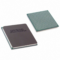
EP1S30F780I6N Altera, EP1S30F780I6N Datasheet - Page 111

EP1S30F780I6N
Manufacturer Part Number
EP1S30F780I6N
Description
IC STRATIX FPGA 30K LE 780-FBGA
Manufacturer
Altera
Series
Stratix®r
Datasheet
1.EP1S10F780C7.pdf
(276 pages)
Specifications of EP1S30F780I6N
Number Of Logic Elements/cells
32470
Number Of Labs/clbs
3247
Total Ram Bits
3317184
Number Of I /o
597
Voltage - Supply
1.425 V ~ 1.575 V
Mounting Type
Surface Mount
Operating Temperature
-40°C ~ 100°C
Package / Case
780-FBGA
Lead Free Status / RoHS Status
Lead free / RoHS Compliant
Number Of Gates
-
Available stocks
Company
Part Number
Manufacturer
Quantity
Price
Company:
Part Number:
EP1S30F780I6N
Manufacturer:
ALTERA
Quantity:
996
- Current page: 111 of 276
- Download datasheet (4Mb)
Altera Corporation
July 2005
VCO period from up to eight taps for individual fine step selection. Also,
each clock output counter can use a unique initial count setting to achieve
individual coarse shift selection in steps of one VCO period. The
combination of coarse and fine shifts allows phase shifting for the entire
input clock period.
The equation to determine the precision of the phase shifting in degrees
is: 45° ÷ post-scale counter value. Therefore, the maximum step size is
45° , and smaller steps are possible depending on the multiplication and
division ratio necessary on the output counter port.
This type of phase shift provides the highest precision since it is the least
sensitive to process, supply, and temperature variation.
Clock Delay
In addition to the phase shift feature, the ability to fine tune the Δt clock
delay provides advanced time delay shift control on each of the four PLL
outputs. There are time delays for each post-scale counter (e, g, or l) from
the PLL, the n counter, and m counter. Each of these can shift in 250-ps
increments for a range of 3.0 ns. The m delay shifts all outputs earlier in
time, while n delay shifts all outputs later in time. Individual delays on
post-scale counters (e, g, and l) provide positive delay for each output.
Table 2–21
delay buffer mode where Δt
The t
delay shift difference between any two PLL outputs, however, must be
less than ±3 ns. For example, shifts on two outputs of –1 and +2 ns is
allowed, but not –1 and +2.5 ns because these shifts would result in a
difference of 3.5 ns. If the design uses external feedback, the Δt
remove delay from outputs, represented by a negative sign (see
Table
feedback loop.
Note to
(1)
Δt
Δt
Δt
Table 2–21. Output Clock Delay for Enhanced PLLs
Normal or Zero Delay Buffer Mode
eOUTPUT
gOUTPUT
lOUTPUT
Δt
OUTPUT
2–21). This effect occurs because the Δt
e
Table
removes delay from outputs in external feedback mode.
= Δt
= Δt
= Δt
shows the combined delay for each output for normal or zero
for a single output can range from –3 ns to +6 ns. The total
n
2–21:
n
n
− Δt
− Δt
− Δt
m
m
m
+ Δt
+ Δt
+ Δt
l
e
g
e
, Δt
g
, or Δt
Δt
Δt
Δt
l
eOUTPUT
gOUTPUT
lOUTPUT
Stratix Device Handbook, Volume 1
is unique for each PLL output.
External Feedback Mode
e
= Δt
delay is then part of the
= Δt
= Δt
n
n
n
− Δt
− Δt
− Δt
m
m
m
Stratix Architecture
+ Δt
− Δt
+ Δt
e
l
g
(1)
e
delay will
2–97
Related parts for EP1S30F780I6N
Image
Part Number
Description
Manufacturer
Datasheet
Request
R

Part Number:
Description:
CYCLONE II STARTER KIT EP2C20N
Manufacturer:
Altera
Datasheet:

Part Number:
Description:
CPLD, EP610 Family, ECMOS Process, 300 Gates, 16 Macro Cells, 16 Reg., 16 User I/Os, 5V Supply, 35 Speed Grade, 24DIP
Manufacturer:
Altera Corporation
Datasheet:

Part Number:
Description:
CPLD, EP610 Family, ECMOS Process, 300 Gates, 16 Macro Cells, 16 Reg., 16 User I/Os, 5V Supply, 15 Speed Grade, 24DIP
Manufacturer:
Altera Corporation
Datasheet:

Part Number:
Description:
Manufacturer:
Altera Corporation
Datasheet:

Part Number:
Description:
CPLD, EP610 Family, ECMOS Process, 300 Gates, 16 Macro Cells, 16 Reg., 16 User I/Os, 5V Supply, 30 Speed Grade, 24DIP
Manufacturer:
Altera Corporation
Datasheet:

Part Number:
Description:
High-performance, low-power erasable programmable logic devices with 8 macrocells, 10ns
Manufacturer:
Altera Corporation
Datasheet:

Part Number:
Description:
High-performance, low-power erasable programmable logic devices with 8 macrocells, 7ns
Manufacturer:
Altera Corporation
Datasheet:

Part Number:
Description:
Classic EPLD
Manufacturer:
Altera Corporation
Datasheet:

Part Number:
Description:
High-performance, low-power erasable programmable logic devices with 8 macrocells, 10ns
Manufacturer:
Altera Corporation
Datasheet:

Part Number:
Description:
Manufacturer:
Altera Corporation
Datasheet:

Part Number:
Description:
Manufacturer:
Altera Corporation
Datasheet:

Part Number:
Description:
Manufacturer:
Altera Corporation
Datasheet:

Part Number:
Description:
CPLD, EP610 Family, ECMOS Process, 300 Gates, 16 Macro Cells, 16 Reg., 16 User I/Os, 5V Supply, 25 Speed Grade, 24DIP
Manufacturer:
Altera Corporation
Datasheet:


