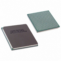
EP1S30F780I6N Altera, EP1S30F780I6N Datasheet - Page 228

EP1S30F780I6N
Manufacturer Part Number
EP1S30F780I6N
Description
IC STRATIX FPGA 30K LE 780-FBGA
Manufacturer
Altera
Series
Stratix®r
Datasheet
1.EP1S10F780C7.pdf
(276 pages)
Specifications of EP1S30F780I6N
Number Of Logic Elements/cells
32470
Number Of Labs/clbs
3247
Total Ram Bits
3317184
Number Of I /o
597
Voltage - Supply
1.425 V ~ 1.575 V
Mounting Type
Surface Mount
Operating Temperature
-40°C ~ 100°C
Package / Case
780-FBGA
Lead Free Status / RoHS Status
Lead free / RoHS Compliant
Number Of Gates
-
Available stocks
Company
Part Number
Manufacturer
Quantity
Price
Company:
Part Number:
EP1S30F780I6N
Manufacturer:
ALTERA
Quantity:
996
- Current page: 228 of 276
- Download datasheet (4Mb)
Timing Model
4–58
Stratix Device Handbook, Volume 1
Figure 4–6
different I/O banks.
Figure 4–6. I/O Skew Across Two I/O Banks
Table 4–97
horizontal I/O pins (side banks 1, 2, 5, 6) and vertical I/O pins (top and
bottom banks 3, 4, 7, 8). The timing parameters define the skew within an
I/O bank, across two neighboring I/O banks on the same side of the
device, across all horizontal I/O banks, across all vertical I/O banks, and
the skew for the overall device.
t
t
t
t
SB_HIO
SB_VIO
SS_HIO
SS_VIO
Table 4–97. Output Pin Timing Skew Definitions (Part 1 of 2)
Symbol
shows the case where four IOE registers are located in two
defines the timing parameters used to define the timing for
I/O Pin A
I/O Pin B
I/O Pin C
I/O Pin D
Row I/O (HIO) within one I/O bank
Column I/O (VIO) within one I/O bank
Row I/O (HIO) same side of the device, across two
banks
Column I/O (VIO) same side of the device, across two
banks
I/O Pin Skew across
(2)
(2)
Common Source of GCLK
I/O Bank
I/O Bank
two Banks
Definition
(1)
Altera Corporation
I/O Pin A
I/O Pin C
I/O Pin B
I/O Pin D
(1)
January 2006
Related parts for EP1S30F780I6N
Image
Part Number
Description
Manufacturer
Datasheet
Request
R

Part Number:
Description:
CYCLONE II STARTER KIT EP2C20N
Manufacturer:
Altera
Datasheet:

Part Number:
Description:
CPLD, EP610 Family, ECMOS Process, 300 Gates, 16 Macro Cells, 16 Reg., 16 User I/Os, 5V Supply, 35 Speed Grade, 24DIP
Manufacturer:
Altera Corporation
Datasheet:

Part Number:
Description:
CPLD, EP610 Family, ECMOS Process, 300 Gates, 16 Macro Cells, 16 Reg., 16 User I/Os, 5V Supply, 15 Speed Grade, 24DIP
Manufacturer:
Altera Corporation
Datasheet:

Part Number:
Description:
Manufacturer:
Altera Corporation
Datasheet:

Part Number:
Description:
CPLD, EP610 Family, ECMOS Process, 300 Gates, 16 Macro Cells, 16 Reg., 16 User I/Os, 5V Supply, 30 Speed Grade, 24DIP
Manufacturer:
Altera Corporation
Datasheet:

Part Number:
Description:
High-performance, low-power erasable programmable logic devices with 8 macrocells, 10ns
Manufacturer:
Altera Corporation
Datasheet:

Part Number:
Description:
High-performance, low-power erasable programmable logic devices with 8 macrocells, 7ns
Manufacturer:
Altera Corporation
Datasheet:

Part Number:
Description:
Classic EPLD
Manufacturer:
Altera Corporation
Datasheet:

Part Number:
Description:
High-performance, low-power erasable programmable logic devices with 8 macrocells, 10ns
Manufacturer:
Altera Corporation
Datasheet:

Part Number:
Description:
Manufacturer:
Altera Corporation
Datasheet:

Part Number:
Description:
Manufacturer:
Altera Corporation
Datasheet:

Part Number:
Description:
Manufacturer:
Altera Corporation
Datasheet:

Part Number:
Description:
CPLD, EP610 Family, ECMOS Process, 300 Gates, 16 Macro Cells, 16 Reg., 16 User I/Os, 5V Supply, 25 Speed Grade, 24DIP
Manufacturer:
Altera Corporation
Datasheet:


