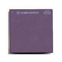
MC68040FE33A Freescale Semiconductor, MC68040FE33A Datasheet - Page 145

MC68040FE33A
Manufacturer Part Number
MC68040FE33A
Description
IC MICROPROCESSOR 32BIT 184-CQFP
Manufacturer
Freescale Semiconductor
Datasheet
1.MC68EC040FE33A.pdf
(442 pages)
Specifications of MC68040FE33A
Processor Type
M680x0 32-Bit
Speed
33MHz
Voltage
5V
Mounting Type
Surface Mount
Package / Case
184-CQFP
Package
184CQFP
Processor Series
M680xx
Core
CPU32
Lead Free Status / RoHS Status
Lead free / RoHS Compliant
Features
-
Lead Free Status / Rohs Status
Details
Available stocks
Company
Part Number
Manufacturer
Quantity
Price
Company:
Part Number:
MC68040FE33A
Manufacturer:
Freescale Semiconductor
Quantity:
10 000
- Current page: 145 of 442
- Download datasheet (4Mb)
Freescale Semiconductor, Inc.
7.2 DATA TRANSFER MECHANISM
Figure 7-2 illustrates how the bus designates operands for transfers on a byte boundary
system. The integer unit handles floating-point operands as a sequence of related long-
word operands. These designations are used in the figures and descriptions that follow.
BYTE 3
BYTE 2
BYTE 1
BYTE 0
31
24 23
16 15
8 7
0
MOST SIGNIFICANT BYTE
LEAST SIGNIFICANT BYTE
LONG-WORD OPERAND
WORD OPERAND
MOST SIGNIFICANT BYTE LEAST SIGNIFICANT BYTE
BYTE OPERAND
Figure 7-2. Internal Operand Representation
Figure 7-3 illustrates general multiplexing between an internal register and the external
bus. The internal register connects to the external data bus through the internal data bus
and multiplexer. The data multiplexer establishes the necessary connections for different
combinations of address and data sizes.
Unlike the MC68020 and MC68030 processors, the M68040 does not support dynamic
bus sizing and expects the referenced device to accept the requested access width. The
MC68150 dynamic bus sizer is designed to allow the 32-bit M68040, MC68EC040,
MC68LC040 bus to communicate bidirectionally with 32-, 16-, or 8-bit peripherals and
memories. It dynamically recognizes the size of the selected peripheral or memory device
and then reads or writes the appropriate data from that location. Refer to MC68150/D,
MC68150 Dynamic Bus Sizer , for information on this device.
Blocks of memory that must be contiguous, such as for code storage or program stacks,
must be 32 bits wide. Byte- and word-sized I/O ports that return an interrupt vector during
interrupt acknowledge cycles must be mapped into the low-order 8 or 16 bits, respectively,
of the data bus.
The multiplexer takes the four bytes of the 32-bit bus transfer and routes them to their
required positions. For example, byte 0 would normally be routed to D31–D24, but it can
also be routed to any other byte position supporting a misaligned data transfer. The same
is true for any of the other operand bytes. The transfer size (SIZ0 and SIZ1) and byte
offset (A1 and A0) signals determine the positioning of the bytes (see Table 7-1). The size
indicated on the SIZx signals corresponds to the size of the operand transfer for the entire
bus cycle. During an operand transfer, A31–A2 indicate the long-word base address for
the first byte of the operand to be accessed; A1 and A0 indicate the byte offset from the
base. For a burst-inhibited line transfer, A1 and A0 for each of the four accesses (the
burst-inhibited line transfer and three long-word transfers) are copied from the lowest two
bits of the access address used to initiate the line transfer.
MOTOROLA
M68040 USER’S MANUAL
7- 3
For More Information On This Product,
Go to: www.freescale.com
Related parts for MC68040FE33A
Image
Part Number
Description
Manufacturer
Datasheet
Request
R

Part Number:
Description:
(MC600 Series) INTEGRATED CIRCUITS
Manufacturer:
ETC
Datasheet:
Part Number:
Description:
Manufacturer:
Freescale Semiconductor, Inc
Datasheet:
Part Number:
Description:
Manufacturer:
Freescale Semiconductor, Inc
Datasheet:
Part Number:
Description:
Manufacturer:
Freescale Semiconductor, Inc
Datasheet:
Part Number:
Description:
Manufacturer:
Freescale Semiconductor, Inc
Datasheet:
Part Number:
Description:
Manufacturer:
Freescale Semiconductor, Inc
Datasheet:
Part Number:
Description:
Manufacturer:
Freescale Semiconductor, Inc
Datasheet:
Part Number:
Description:
Manufacturer:
Freescale Semiconductor, Inc
Datasheet:
Part Number:
Description:
Manufacturer:
Freescale Semiconductor, Inc
Datasheet:
Part Number:
Description:
Manufacturer:
Freescale Semiconductor, Inc
Datasheet:
Part Number:
Description:
Manufacturer:
Freescale Semiconductor, Inc
Datasheet:
Part Number:
Description:
Manufacturer:
Freescale Semiconductor, Inc
Datasheet:
Part Number:
Description:
Manufacturer:
Freescale Semiconductor, Inc
Datasheet:
Part Number:
Description:
Manufacturer:
Freescale Semiconductor, Inc
Datasheet:
Part Number:
Description:
Manufacturer:
Freescale Semiconductor, Inc
Datasheet:


