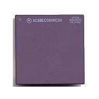
MC68040FE33A Freescale Semiconductor, MC68040FE33A Datasheet - Page 148

MC68040FE33A
Manufacturer Part Number
MC68040FE33A
Description
IC MICROPROCESSOR 32BIT 184-CQFP
Manufacturer
Freescale Semiconductor
Datasheet
1.MC68EC040FE33A.pdf
(442 pages)
Specifications of MC68040FE33A
Processor Type
M680x0 32-Bit
Speed
33MHz
Voltage
5V
Mounting Type
Surface Mount
Package / Case
184-CQFP
Package
184CQFP
Processor Series
M680xx
Core
CPU32
Lead Free Status / RoHS Status
Lead free / RoHS Compliant
Features
-
Lead Free Status / Rohs Status
Details
Available stocks
Company
Part Number
Manufacturer
Quantity
Price
Company:
Part Number:
MC68040FE33A
Manufacturer:
Freescale Semiconductor
Quantity:
10 000
- Current page: 148 of 442
- Download datasheet (4Mb)
7.3 MISALIGNED OPERANDS
All M68040 data formats can be located in memory on any byte boundary. A byte operand
is properly aligned at any address; a word operand is misaligned at an odd address; and a
long word is misaligned at an address that is not evenly divisible by 4. However, since
operands can reside at any byte boundary, they can be misaligned. Although the M68040
does not enforce any alignment restrictions for data operands (including PC relative data
addressing), some performance degradation occurs when additional bus cycles are
required for long-word or word operands that are misaligned. For maximum performance,
data items should be aligned on their natural boundaries. All instruction words and
extension words must reside on word boundaries. Attempting to prefetch an instruction
word at an odd address causes an address error exception. Refer to Section 8 Exception
Processing for details on address error exceptions.
The M68040 data memory unit converts misaligned operand accesses that are
noncachable to a sequence of aligned accesses. These aligned accesses are then sent to
the bus controller for completion, always resulting in aligned bus transfers. Misaligned
operand accesses that miss in the data cache are cachable and are not aligned before
line filling. Refer to Section 4 Instruction and Data Caches for details on line fill and the
data cache.
7-6
NOTES
UPA1, UPA0
TLN1, TLN0
SIZ1, SIZ0
TM4–TM2
1. The UPA1, UPA0, and CIOUT signals are determined by the U1, U0 data and CM bit fields, respectively,
2. The TLNx signals are defined only for normal push accesses and normal data line read accesses.
3. The LOCK signal is asserted during TAS, CAS, and CAS2 operand accesses and for some table search update
4. Refer to Section 5 Signal Description for definitions of the TMx signal encodings for normal, MOVE16,
TT1, TT0
A31–A0
LOCKE
Signal
CIOUT
LOCK
Bus
R/ W
corresponding to the access address.
sequences. LOCKE is asserted for the last transfer of each locked sequence of transfers.
and alternate accesses.
Table 7-2. Summary of Access Types versus Bus Signal Encodings
Data Cache
Cache Set
Address
Negated
Negated
Access
Access
L/Line
Push
Entry
Write
$0
$0
$0
$1,2,5, or 6
Data/Code
Read/Write
B/W/L/Line
Cache Set
Asserted/
Negated 3
Source 1
Source 1
Access
Address
Freescale Semiconductor, Inc.
Normal
Access
Entry 2
MMU
MMU
$0
For More Information On This Product,
M68040 USER’S MANUAL
Read/Write
Go to: www.freescale.com
Long Word
Undefined
Negated 3
Asserted/
Address
Negated
Access
Search
$3 or 4
Table
Entry
$0
$0
Read/Write
Undefined
MOVE16
Source 1
Negated
Source 1
Access
Address
Access
$1 or 5
MMU
MMU
Line
$1
Read/Write
Undefined
Alternate
Asserted
Function
Negated
Access
Address
Access
B/W/L
Code
$0
$2
Acknowledge
Int. Level $1–7
$FFFFFFFF
Undefined
Interrupt
Negated
Negated
Read
Byte
$0
$3
Acknowledge
MOTOROLA
Breakpoint
$00000000
Undefined
Negated
Negated
Read
Byte
$0
$3
$0
Related parts for MC68040FE33A
Image
Part Number
Description
Manufacturer
Datasheet
Request
R

Part Number:
Description:
(MC600 Series) INTEGRATED CIRCUITS
Manufacturer:
ETC
Datasheet:
Part Number:
Description:
Manufacturer:
Freescale Semiconductor, Inc
Datasheet:
Part Number:
Description:
Manufacturer:
Freescale Semiconductor, Inc
Datasheet:
Part Number:
Description:
Manufacturer:
Freescale Semiconductor, Inc
Datasheet:
Part Number:
Description:
Manufacturer:
Freescale Semiconductor, Inc
Datasheet:
Part Number:
Description:
Manufacturer:
Freescale Semiconductor, Inc
Datasheet:
Part Number:
Description:
Manufacturer:
Freescale Semiconductor, Inc
Datasheet:
Part Number:
Description:
Manufacturer:
Freescale Semiconductor, Inc
Datasheet:
Part Number:
Description:
Manufacturer:
Freescale Semiconductor, Inc
Datasheet:
Part Number:
Description:
Manufacturer:
Freescale Semiconductor, Inc
Datasheet:
Part Number:
Description:
Manufacturer:
Freescale Semiconductor, Inc
Datasheet:
Part Number:
Description:
Manufacturer:
Freescale Semiconductor, Inc
Datasheet:
Part Number:
Description:
Manufacturer:
Freescale Semiconductor, Inc
Datasheet:
Part Number:
Description:
Manufacturer:
Freescale Semiconductor, Inc
Datasheet:
Part Number:
Description:
Manufacturer:
Freescale Semiconductor, Inc
Datasheet:


