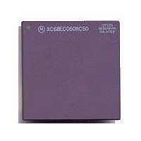
MC68040FE33A Freescale Semiconductor, MC68040FE33A Datasheet - Page 155

MC68040FE33A
Manufacturer Part Number
MC68040FE33A
Description
IC MICROPROCESSOR 32BIT 184-CQFP
Manufacturer
Freescale Semiconductor
Datasheet
1.MC68EC040FE33A.pdf
(442 pages)
Specifications of MC68040FE33A
Processor Type
M680x0 32-Bit
Speed
33MHz
Voltage
5V
Mounting Type
Surface Mount
Package / Case
184-CQFP
Package
184CQFP
Processor Series
M680xx
Core
CPU32
Lead Free Status / RoHS Status
Lead free / RoHS Compliant
Features
-
Lead Free Status / Rohs Status
Details
Available stocks
Company
Part Number
Manufacturer
Quantity
Price
Company:
Part Number:
MC68040FE33A
Manufacturer:
Freescale Semiconductor
Quantity:
10 000
- Current page: 155 of 442
- Download datasheet (4Mb)
Freescale Semiconductor, Inc.
the data bus and asserting TA. A line transfer performed in this manner with a single
address is referred to as a line burst transfer.
The M68040 also supports burst-inhibited line transfers for memory devices that are
unable to support bursting. For this type of bus cycle, the selected device supplies the first
long word pointed to by the processor address and asserts transfer burst inhibit (TBI) with
TA for the first transfer of the line access. The processor responds by terminating the line
burst transfer and accessing the remainder of the line, using three long-word read bus
cycles. Although the selected device can then treat the line transfer as four, independent,
long-word bus cycles, the bus controller still handles the four transfers as a single line
transfer and does not allow other unrelated processor accesses or bus arbitration to
intervene between the transfers. TBI is ignored after the first long-word transfer.
Line reads to support cache line filling can be cache inhibited by asserting transfer cache
inhibit (TCI) with TA for the first long-word transfer of the line. The assertion of TCI does
not affect completion of the line transfer, but the bus controller latches and passes it to the
memory controller for use. TCI is ignored after the first long-word transfer of a line burst
transfer and during the three long-word bus cycles for a burst-inhibited line transfer.
The address placed on the address bus by the processor for line transfers does not
necessarily point to the most significant byte of each long word because for a line read, A1
and A0 are copied from the original operand address supplied to the memory unit by the
integer unit. These two bits are also unchanged for the three long-word bus cycles for a
burst-inhibited line transfer. The selected device should ignore A1 and A0 for long-word
and line read transfers.
The address of an instruction fetch will always be aligned to a half-line boundary
($XXXXXXX0 or $XXXXXXX8); therefore, compilers should attempt to locate branch
targets on half-line boundaries to minimize branch stalls. For example, if the target of a
branch is a two-word instruction located at $1000000C, the following burst sequence will
occur upon a cache miss: $10000008, $1000000C, $10000000, then $10000004. The
internal pipeline of the M68040 stalls until the second access of the burst (the address of
the instruction to be executed) has completed. Figures 7-10 and 7-11 illustrate a flowchart
and functional timing diagram for a line read bus transfer.
MOTOROLA
M68040 USER’S MANUAL
7- 13
For More Information On This Product,
Go to: www.freescale.com
Related parts for MC68040FE33A
Image
Part Number
Description
Manufacturer
Datasheet
Request
R

Part Number:
Description:
(MC600 Series) INTEGRATED CIRCUITS
Manufacturer:
ETC
Datasheet:
Part Number:
Description:
Manufacturer:
Freescale Semiconductor, Inc
Datasheet:
Part Number:
Description:
Manufacturer:
Freescale Semiconductor, Inc
Datasheet:
Part Number:
Description:
Manufacturer:
Freescale Semiconductor, Inc
Datasheet:
Part Number:
Description:
Manufacturer:
Freescale Semiconductor, Inc
Datasheet:
Part Number:
Description:
Manufacturer:
Freescale Semiconductor, Inc
Datasheet:
Part Number:
Description:
Manufacturer:
Freescale Semiconductor, Inc
Datasheet:
Part Number:
Description:
Manufacturer:
Freescale Semiconductor, Inc
Datasheet:
Part Number:
Description:
Manufacturer:
Freescale Semiconductor, Inc
Datasheet:
Part Number:
Description:
Manufacturer:
Freescale Semiconductor, Inc
Datasheet:
Part Number:
Description:
Manufacturer:
Freescale Semiconductor, Inc
Datasheet:
Part Number:
Description:
Manufacturer:
Freescale Semiconductor, Inc
Datasheet:
Part Number:
Description:
Manufacturer:
Freescale Semiconductor, Inc
Datasheet:
Part Number:
Description:
Manufacturer:
Freescale Semiconductor, Inc
Datasheet:
Part Number:
Description:
Manufacturer:
Freescale Semiconductor, Inc
Datasheet:


