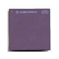
MC68040FE33A Freescale Semiconductor, MC68040FE33A Datasheet - Page 158

MC68040FE33A
Manufacturer Part Number
MC68040FE33A
Description
IC MICROPROCESSOR 32BIT 184-CQFP
Manufacturer
Freescale Semiconductor
Datasheet
1.MC68EC040FE33A.pdf
(442 pages)
Specifications of MC68040FE33A
Processor Type
M680x0 32-Bit
Speed
33MHz
Voltage
5V
Mounting Type
Surface Mount
Package / Case
184-CQFP
Package
184CQFP
Processor Series
M680xx
Core
CPU32
Lead Free Status / RoHS Status
Lead free / RoHS Compliant
Features
-
Lead Free Status / Rohs Status
Details
Available stocks
Company
Part Number
Manufacturer
Quantity
Price
Company:
Part Number:
MC68040FE33A
Manufacturer:
Freescale Semiconductor
Quantity:
10 000
- Current page: 158 of 442
- Download datasheet (4Mb)
Clock 2 (C2)
Clock 3 (C3)
Clock 4 (C4)
7-16
(Except MC68EC040 and MC68EC040V) for information on the M68040 and
MC68LC040 memory units and Appendix B MC68EC040 for information on the
MC68EC040 memory unit.
The processor asserts TS during C1 to indicate the beginning of a bus cycle. If not
already asserted from a previous bus cycle, TIP is also asserted at this time to indicate
that a bus cycle is active.
During the first half of the first clock after C1, the processor negates TS. The selected
device uses R/W, SIZ1, and SIZ0 to place the data on the data bus. (The first transfer
must supply the long word at the corresponding long-word boundary.) Concurrently, the
selected device asserts TA and either negates or asserts TBI to indicate it can or cannot
support a burst transfer. At the end of the first clock cycle after C1, the processor
samples the level of TA, TBI, and TCI and latches the current value on the data bus. If
TA is asserted, the transfer terminates and the data is passed to the appropriate
memory unit. If TA is not recognized asserted, the processor ignores the data and
inserts wait states instead of terminating the transfer. The processor continues to
sample TA, TBI, and TCI on successive rising edges of BCLK until TA is recognized
asserted. The latched data and the level on TCI are then passed to the appropriate
memory unit.
If TBI was negated with TA, the processor continues the cycle with C3. Otherwise, if TBI
was asserted, the line transfer is burst inhibited, and the processor reads the remaining
three long words using long-word read bus cycles. The processor increments A3 and
A2 for each read, and the new address is placed on the address bus for each bus cycle.
Refer to 7.4.1 Byte, Word, and Long-Word Read Transfers for information on long-
word reads. If no wait states are generated, a burst-inhibited line read completes in
eight clocks instead of the five required for a burst read.
The processor holds the address and transfer attribute signals constant during C3. The
selected device must increment A3 and A2 to reference the next long word to transfer,
place the data on the data bus, and assert TA. At the end of C3, the processor samples
the level of TA and latches the current value on the data bus. If TA is asserted, the
transfer terminates, and the second long word of data is passed to the appropriate
memory unit. If TA is not recognized asserted at the end of C3, the processor ignores
the latched data and inserts wait states instead of terminating the transfer. The
processor continues to sample TA on successive rising edges of BCLK until it is
recognized. The latched data is then passed to the appropriate memory unit.
This clock is identical to C3 except that once TA is recognized asserted, the latched
value corresponds to the third long word of data for the burst.
Freescale Semiconductor, Inc.
For More Information On This Product,
M68040 USER’S MANUAL
Go to: www.freescale.com
MOTOROLA
Related parts for MC68040FE33A
Image
Part Number
Description
Manufacturer
Datasheet
Request
R

Part Number:
Description:
(MC600 Series) INTEGRATED CIRCUITS
Manufacturer:
ETC
Datasheet:
Part Number:
Description:
Manufacturer:
Freescale Semiconductor, Inc
Datasheet:
Part Number:
Description:
Manufacturer:
Freescale Semiconductor, Inc
Datasheet:
Part Number:
Description:
Manufacturer:
Freescale Semiconductor, Inc
Datasheet:
Part Number:
Description:
Manufacturer:
Freescale Semiconductor, Inc
Datasheet:
Part Number:
Description:
Manufacturer:
Freescale Semiconductor, Inc
Datasheet:
Part Number:
Description:
Manufacturer:
Freescale Semiconductor, Inc
Datasheet:
Part Number:
Description:
Manufacturer:
Freescale Semiconductor, Inc
Datasheet:
Part Number:
Description:
Manufacturer:
Freescale Semiconductor, Inc
Datasheet:
Part Number:
Description:
Manufacturer:
Freescale Semiconductor, Inc
Datasheet:
Part Number:
Description:
Manufacturer:
Freescale Semiconductor, Inc
Datasheet:
Part Number:
Description:
Manufacturer:
Freescale Semiconductor, Inc
Datasheet:
Part Number:
Description:
Manufacturer:
Freescale Semiconductor, Inc
Datasheet:
Part Number:
Description:
Manufacturer:
Freescale Semiconductor, Inc
Datasheet:
Part Number:
Description:
Manufacturer:
Freescale Semiconductor, Inc
Datasheet:


