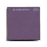
MC68040FE33A Freescale Semiconductor, MC68040FE33A Datasheet - Page 16

MC68040FE33A
Manufacturer Part Number
MC68040FE33A
Description
IC MICROPROCESSOR 32BIT 184-CQFP
Manufacturer
Freescale Semiconductor
Datasheet
1.MC68EC040FE33A.pdf
(442 pages)
Specifications of MC68040FE33A
Processor Type
M680x0 32-Bit
Speed
33MHz
Voltage
5V
Mounting Type
Surface Mount
Package / Case
184-CQFP
Package
184CQFP
Processor Series
M680xx
Core
CPU32
Lead Free Status / RoHS Status
Lead free / RoHS Compliant
Features
-
Lead Free Status / Rohs Status
Details
Available stocks
Company
Part Number
Manufacturer
Quantity
Price
Company:
Part Number:
MC68040FE33A
Manufacturer:
Freescale Semiconductor
Quantity:
10 000
- Current page: 16 of 442
- Download datasheet (4Mb)
4-5
4-6
5-1
6-1
6-2
6-3
6-4
6-5
6-6
6-7
6-8
6-9
6-10
6-11
7-1
7-2
7-3
7-4
7-5
7-6
7-7
7-8
7-9
7-10
7-11
7-12
7-13
7-14
7-15
7-16
7-17
7-18
7-19
7-20
7-21
7-22
7-23
7-24
7-25
xviii
Number
Figure
Instruction-Cache Line State Diagram ......................................................... 4-14
Data-Cache Line State Diagram .................................................................. 4-16
Functional Signal Groups ............................................................................. 5-4
M68040 Test Logic Block Diagram .............................................................. 6-2
Bypass Register ........................................................................................... 6-6
Output Latch Cell (O.Latch) ......................................................................... 6-7
Input Pin Cell (I.Pin) ..................................................................................... 6-7
Output Control Cells (IO.Ctl) ........................................................................ 6-8
General Arrangement of Bidirectional Pins .................................................. 6-8
Circuit Disabling IEEE Standard 1149.1A .................................................... 6-14
Clock Input Timing Diagram ......................................................................... 6-22
TRST Timing Diagram .................................................................................. 6-22
Boundary Scan Timing Diagram .................................................................. 6-23
Test Access Port Timing Diagram ............................................................... 6-23
Signal Relationships to Clocks..................................................................... 7-2
Internal Operand Representation ................................................................. 7-3
Data Multiplexing ......................................................................................... 7-4
Byte Enable Signal Generation and PAL Equation ...................................... 7-5
Example of a Misaligned Long-Word Transfer............................................. 7-7
Example of a Misaligned Word Transfer ...................................................... 7-7
Misaligned Long-Word Read Transfer Timing ............................................. 7-8
Byte, Word, and Long-Word Read Transfer Flowchart ................................ 7-10
Byte, Word, and Long-Word Read Transfer Timing..................................... 7-11
Line Read Transfer Flowchart...................................................................... 7-14
Line Read Transfer Timing .......................................................................... 7-15
Burst-Inhibited Line Read Transfer Flowchart ............................................. 7-18
Burst-Inhibited Line Read Transfer Timing .................................................. 7-19
Byte, Word, and Long-Word Write Transfer Flowchart ................................ 7-20
Long-Word Write Transfer Timing ................................................................ 7-21
Line Write Transfer Flowchart ...................................................................... 7-23
Line Write Transfer Timing........................................................................... 7-24
Locked Transfer for TAS Instruction Timing ................................................ 7-27
Interrupt Pending Procedure ........................................................................ 7-30
Assertion of IPEND ...................................................................................... 7-30
Interrupt Acknowledge Bus Cycle Flowchart ............................................... 7-32
Interrupt Acknowledge Bus Cycle Timing .................................................... 7-33
Autovector Interrupt Acknowledge Bus Cycle Timing .................................. 7-34
Breakpoint Interrupt Acknowledge Bus Cycle Flowchart ............................. 7-35
Breakpoint Interrupt Acknowledge Bus Cycle Timing .................................. 7-36
LIST OF ILLUSTRATIONS (Continued)
Freescale Semiconductor, Inc.
For More Information On This Product,
M68040 USER’S MANUAL
Go to: www.freescale.com
Title
MOTOROLA
Number
Page
Related parts for MC68040FE33A
Image
Part Number
Description
Manufacturer
Datasheet
Request
R

Part Number:
Description:
(MC600 Series) INTEGRATED CIRCUITS
Manufacturer:
ETC
Datasheet:
Part Number:
Description:
Manufacturer:
Freescale Semiconductor, Inc
Datasheet:
Part Number:
Description:
Manufacturer:
Freescale Semiconductor, Inc
Datasheet:
Part Number:
Description:
Manufacturer:
Freescale Semiconductor, Inc
Datasheet:
Part Number:
Description:
Manufacturer:
Freescale Semiconductor, Inc
Datasheet:
Part Number:
Description:
Manufacturer:
Freescale Semiconductor, Inc
Datasheet:
Part Number:
Description:
Manufacturer:
Freescale Semiconductor, Inc
Datasheet:
Part Number:
Description:
Manufacturer:
Freescale Semiconductor, Inc
Datasheet:
Part Number:
Description:
Manufacturer:
Freescale Semiconductor, Inc
Datasheet:
Part Number:
Description:
Manufacturer:
Freescale Semiconductor, Inc
Datasheet:
Part Number:
Description:
Manufacturer:
Freescale Semiconductor, Inc
Datasheet:
Part Number:
Description:
Manufacturer:
Freescale Semiconductor, Inc
Datasheet:
Part Number:
Description:
Manufacturer:
Freescale Semiconductor, Inc
Datasheet:
Part Number:
Description:
Manufacturer:
Freescale Semiconductor, Inc
Datasheet:
Part Number:
Description:
Manufacturer:
Freescale Semiconductor, Inc
Datasheet:


