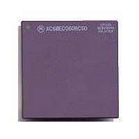
MC68040FE33A Freescale Semiconductor, MC68040FE33A Datasheet - Page 239

MC68040FE33A
Manufacturer Part Number
MC68040FE33A
Description
IC MICROPROCESSOR 32BIT 184-CQFP
Manufacturer
Freescale Semiconductor
Datasheet
1.MC68EC040FE33A.pdf
(442 pages)
Specifications of MC68040FE33A
Processor Type
M680x0 32-Bit
Speed
33MHz
Voltage
5V
Mounting Type
Surface Mount
Package / Case
184-CQFP
Package
184CQFP
Processor Series
M680xx
Core
CPU32
Lead Free Status / RoHS Status
Lead free / RoHS Compliant
Features
-
Lead Free Status / Rohs Status
Details
Available stocks
Company
Part Number
Manufacturer
Quantity
Price
Company:
Part Number:
MC68040FE33A
Manufacturer:
Freescale Semiconductor
Quantity:
10 000
- Current page: 239 of 442
- Download datasheet (4Mb)
ATC—ATC Fault
LK—Locked Transfer (Read-Modify-Write)
RW—Read/Write
X—Undefined
SIZE—Transfer Size
TT—Transfer Type
TM—Transfer Modifier
8.4.6.3 WRITE-BACK STATUS. These fields contain status information for the three
possible write-backs that could be pending after the faulted access (see Figure 8-8). For a
data cache line-push fault or a MOVE16 write fault, WB1S is zero (invalid).
8.4.6.4 FAULT ADDRESS. The fault address (FA) is the initial address for the access that
faulted. The FA is a physical address only for cache pushes and a logical address for all
other cases. For a misaligned access that faults, the FA field contains the address of the
first byte of the transfer, regardless of which of the two or three bus transfers for the
misaligned access was faulted. For a push fault, the WB1A and FA addresses are the
same.
8.4.6.5 WRITE-BACK ADDRESS AND WRITE-BACK DATA. Write-back addresses
(WB3A, WB2A, and WB1A) are memory pointers that indicate where to place the write-
8-26
This bit is set for an ATC fault due to a nonresident entry (bus error during table search
or invalid descriptor encountered) or privilege violation (write protected or supervisor
only). It is cleared for a bus-errored instruction, data, or cache line-push access.
This bit is set if a fault occurred on a locked transfer; it is cleared otherwise.
This bit is set if a fault occurred on a read transfer; it is cleared otherwise.
The SIZE field corresponds to the original access size. If a data cache line read results
from a read miss and the line read encounters a bus error, the SIZE field in the resulting
stack frame indicates the size of the original read generated by the execution unit.
This field defines the TT1–TT0 signal encodings for the faulted transfer.
This field defines the TM2–TM0 signal encodings for the faulted transfer.
TM—Transfer Modifier
TT—Transfer Type
SIZE—Transfer Size
V—Valid Write (write-back pending if set)
Freescale Semiconductor, Inc.
7
V
Figure 8-8. Write-Back Status Format
For More Information On This Product,
6
SIZE
M68040 USER’S MANUAL
Go to: www.freescale.com
5
4
TT
3
2
TM
1
0
MOTOROLA
Related parts for MC68040FE33A
Image
Part Number
Description
Manufacturer
Datasheet
Request
R

Part Number:
Description:
(MC600 Series) INTEGRATED CIRCUITS
Manufacturer:
ETC
Datasheet:
Part Number:
Description:
Manufacturer:
Freescale Semiconductor, Inc
Datasheet:
Part Number:
Description:
Manufacturer:
Freescale Semiconductor, Inc
Datasheet:
Part Number:
Description:
Manufacturer:
Freescale Semiconductor, Inc
Datasheet:
Part Number:
Description:
Manufacturer:
Freescale Semiconductor, Inc
Datasheet:
Part Number:
Description:
Manufacturer:
Freescale Semiconductor, Inc
Datasheet:
Part Number:
Description:
Manufacturer:
Freescale Semiconductor, Inc
Datasheet:
Part Number:
Description:
Manufacturer:
Freescale Semiconductor, Inc
Datasheet:
Part Number:
Description:
Manufacturer:
Freescale Semiconductor, Inc
Datasheet:
Part Number:
Description:
Manufacturer:
Freescale Semiconductor, Inc
Datasheet:
Part Number:
Description:
Manufacturer:
Freescale Semiconductor, Inc
Datasheet:
Part Number:
Description:
Manufacturer:
Freescale Semiconductor, Inc
Datasheet:
Part Number:
Description:
Manufacturer:
Freescale Semiconductor, Inc
Datasheet:
Part Number:
Description:
Manufacturer:
Freescale Semiconductor, Inc
Datasheet:
Part Number:
Description:
Manufacturer:
Freescale Semiconductor, Inc
Datasheet:


