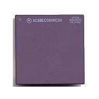
MC68040FE33A Freescale Semiconductor, MC68040FE33A Datasheet - Page 361

MC68040FE33A
Manufacturer Part Number
MC68040FE33A
Description
IC MICROPROCESSOR 32BIT 184-CQFP
Manufacturer
Freescale Semiconductor
Datasheet
1.MC68EC040FE33A.pdf
(442 pages)
Specifications of MC68040FE33A
Processor Type
M680x0 32-Bit
Speed
33MHz
Voltage
5V
Mounting Type
Surface Mount
Package / Case
184-CQFP
Package
184CQFP
Processor Series
M680xx
Core
CPU32
Lead Free Status / RoHS Status
Lead free / RoHS Compliant
Features
-
Lead Free Status / Rohs Status
Details
Available stocks
Company
Part Number
Manufacturer
Quantity
Price
Company:
Part Number:
MC68040FE33A
Manufacturer:
Freescale Semiconductor
Quantity:
10 000
- Current page: 361 of 442
- Download datasheet (4Mb)
APPENDIX A
MC68LC040
The MC68LC040 is Motorola's integer-only version of the MC68040 third-generation,
M68000-compatible, high-performance, 32-bit microprocessor. The MC68LC040 is a virtual
memory microprocessor with a highly integrated architecture that provides very high perfor-
mance in a monolithic HCMOS device. On a single chip, the MC68LC040 integrates an
MC68040-compatible integer unit and fully independent instruction and data demand-paged
memory management units (MMUs), including independent 4-Kbyte instruction and data
caches. A high degree of instruction execution parallelism is achieved through the use of a
six-stage instruction pipeline, multiple internal buses, and a full internal Harvard architec-
ture, including separate physical caches for both instruction and data accesses. The
MC68LC040 also directly supports cache coherency in multimaster applications with dedi-
cated on-chip bus snooping logic.
The MC68LC040 achieves its high performance through the use of the MC68040 integer
unit. The six-stage pipeline operates on up to six instructions concurrent with MMU, cache,
and bus controller operations. Multiple internal buses, separate data and instruction caches,
and a sophisticated bus controller allow internal units to operate concurrently and decouple
the MC68LC040 from the external bus. The internal caches and the decoupling of the exter-
nal bus allow for an external memory subsystem to be built from slower and less expensive
memories with minimal impact to the overall system performance. The potential for a
low-cost system design with the price/performance of the MC68LC040 makes it a good
choice for embedded microprocessor applications as well as central processor applications.
The MC68LC040 is user-object-code compatible with previous members of the M68000
family and is specifically optimized to reduce the execution time of compiler-generated code.
The high level of performance is ideal for integer-intensive applications. The MC68LC040 is
implemented in Motorola's latest HCMOS technology, providing an ideal balance between
speed, power, and physical device size. Independent data and instruction MMUs control the
main caches and the address translation caches (ATCs). The ATCs speed up logi-
cal-to-physical address translations by storing recently used translations. The bus snooper
circuit ensures cache coherency in multimaster and multiprocessing applications. The
MOTOROLA
Rev. 2.3 contains timing informationg for 40 MHz operation.
Refer to chang bars for these additions.
All references to MC68LC040 also apply to the MC68040V.
Refer to Appendix C MC68040V and MC68EC040V for more
information on the MC68040V.
Freescale Semiconductor, Inc.
For More Information On This Product,
Go to: www.freescale.com
M68040 USER’S MANUAL
NOTE
REV2.3 (01/29/2000)
A-1
Related parts for MC68040FE33A
Image
Part Number
Description
Manufacturer
Datasheet
Request
R

Part Number:
Description:
(MC600 Series) INTEGRATED CIRCUITS
Manufacturer:
ETC
Datasheet:
Part Number:
Description:
Manufacturer:
Freescale Semiconductor, Inc
Datasheet:
Part Number:
Description:
Manufacturer:
Freescale Semiconductor, Inc
Datasheet:
Part Number:
Description:
Manufacturer:
Freescale Semiconductor, Inc
Datasheet:
Part Number:
Description:
Manufacturer:
Freescale Semiconductor, Inc
Datasheet:
Part Number:
Description:
Manufacturer:
Freescale Semiconductor, Inc
Datasheet:
Part Number:
Description:
Manufacturer:
Freescale Semiconductor, Inc
Datasheet:
Part Number:
Description:
Manufacturer:
Freescale Semiconductor, Inc
Datasheet:
Part Number:
Description:
Manufacturer:
Freescale Semiconductor, Inc
Datasheet:
Part Number:
Description:
Manufacturer:
Freescale Semiconductor, Inc
Datasheet:
Part Number:
Description:
Manufacturer:
Freescale Semiconductor, Inc
Datasheet:
Part Number:
Description:
Manufacturer:
Freescale Semiconductor, Inc
Datasheet:
Part Number:
Description:
Manufacturer:
Freescale Semiconductor, Inc
Datasheet:
Part Number:
Description:
Manufacturer:
Freescale Semiconductor, Inc
Datasheet:
Part Number:
Description:
Manufacturer:
Freescale Semiconductor, Inc
Datasheet:


