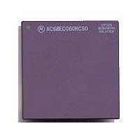
MC68040FE33A Freescale Semiconductor, MC68040FE33A Datasheet - Page 383

MC68040FE33A
Manufacturer Part Number
MC68040FE33A
Description
IC MICROPROCESSOR 32BIT 184-CQFP
Manufacturer
Freescale Semiconductor
Datasheet
1.MC68EC040FE33A.pdf
(442 pages)
Specifications of MC68040FE33A
Processor Type
M680x0 32-Bit
Speed
33MHz
Voltage
5V
Mounting Type
Surface Mount
Package / Case
184-CQFP
Package
184CQFP
Processor Series
M680xx
Core
CPU32
Lead Free Status / RoHS Status
Lead free / RoHS Compliant
Features
-
Lead Free Status / Rohs Status
Details
Available stocks
Company
Part Number
Manufacturer
Quantity
Price
Company:
Part Number:
MC68040FE33A
Manufacturer:
Freescale Semiconductor
Quantity:
10 000
- Current page: 383 of 442
- Download datasheet (4Mb)
Freescale Semiconductor, Inc.
MC68EC040
REV2.3 (01/31/2000)
ADDRESS MASK field equals $0F, the W-bit is set to one, and the S-field = $1. The inclusion
of independent ACRs in both the instruction ACU (IACU) and data ACU (DACU provides an
exception to the merged instruction and data address space, allowing different access con-
trol for instruction and operand accesses. Also, since the instruction memory unit is only
used for instruction prefetches, different instruction and data ACRs can cause PC relative
operand fetches to be translated differently from instruction prefetches.
Matching either of the ACRs in a corresponding ACU during an access to a memory unit
completes the access with the ACU. If both registers match, the access uses the xACR0 sta-
tus bits. Addresses are passed through without translation if there is no match in the ACRs
and no table search occurs. The MC68EC040 does not perform table searches.
B.3.3 Effect of RSTI on the ACU
When the assertion of the reset input (RSTI) signal resets the MC68EC040, the E-bits of the
ACRs are cleared, disabling address access control.
B.4 SPECIAL MODES OF OPERATION
This part of the M68040 User's Manual does not apply to the MC68EC040. The
MC68EC040 does not sample the IPL2–IPL0, CDIS, JS0 (DLE on the MC68040), or JS1
(MDIS on the MC68040) pins on the rising edge of RSTI.
An external device asserts RSTI to reset the processor. When power is applied to the sys-
tem, external circuitry should assert RSTI for a minimum of 10 BCLK cycles after V
is
CC
within tolerance. Figure B-5 is a functional timing diagram of the power-on reset operation,
illustrating the relationships between V
, RSTI, and bus signals. The BCLK and PCLK
CC
clock signals are required to be stable by the time V
reaches the minimum operating spec-
CC
ification. RSTI is internally synchronized for two BCLKS before being used, and must meet
the specified setup and hold times to BCLK (specifications #51 and #52 in MC68EC040
Electrical Characteristics ) only if recognition by a specific BCLK rising edge is required.
Once RSTI is negated, the processor is internally held in reset for another 128 clock cycles.
During the reset period, all three-statable signals are three-stated, and the rest are driven to
their inactive state. Once the internal reset signal negates, all bus signals remain in a
high-impedance state until the processor is granted the bus. After this, the first bus cycle for
reset exception processing begins. In Figure B-6, the processor assumes implicit ownership
of the bus before the first bus cycle begins. The levels on the CDIS, JS1 (MDIS on the
MC68040), and IPL2–IPL0 signals are not sampled when RSTI is negated.
For processor resets after the initial power-on reset, should be asserted for at least 10 clock
periods. Figure B-6 illustrates timing associated with a reset when the processor is executing
bus cycles. Note that BB and TIP (and TA driven during a snooped access) are asserted
before transitioning to a three-state level. Processor reset causes any bus cycle in progress
to terminate as if TA or TEA had been asserted. Also, the processor initializes registers
appropriately for a reset exception.
MOTOROLA
M68040 USER’S MANUAL
B-7
For More Information On This Product,
Go to: www.freescale.com
Related parts for MC68040FE33A
Image
Part Number
Description
Manufacturer
Datasheet
Request
R

Part Number:
Description:
(MC600 Series) INTEGRATED CIRCUITS
Manufacturer:
ETC
Datasheet:
Part Number:
Description:
Manufacturer:
Freescale Semiconductor, Inc
Datasheet:
Part Number:
Description:
Manufacturer:
Freescale Semiconductor, Inc
Datasheet:
Part Number:
Description:
Manufacturer:
Freescale Semiconductor, Inc
Datasheet:
Part Number:
Description:
Manufacturer:
Freescale Semiconductor, Inc
Datasheet:
Part Number:
Description:
Manufacturer:
Freescale Semiconductor, Inc
Datasheet:
Part Number:
Description:
Manufacturer:
Freescale Semiconductor, Inc
Datasheet:
Part Number:
Description:
Manufacturer:
Freescale Semiconductor, Inc
Datasheet:
Part Number:
Description:
Manufacturer:
Freescale Semiconductor, Inc
Datasheet:
Part Number:
Description:
Manufacturer:
Freescale Semiconductor, Inc
Datasheet:
Part Number:
Description:
Manufacturer:
Freescale Semiconductor, Inc
Datasheet:
Part Number:
Description:
Manufacturer:
Freescale Semiconductor, Inc
Datasheet:
Part Number:
Description:
Manufacturer:
Freescale Semiconductor, Inc
Datasheet:
Part Number:
Description:
Manufacturer:
Freescale Semiconductor, Inc
Datasheet:
Part Number:
Description:
Manufacturer:
Freescale Semiconductor, Inc
Datasheet:


