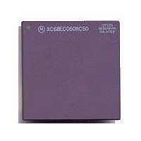
MC68040FE33A Freescale Semiconductor, MC68040FE33A Datasheet - Page 409

MC68040FE33A
Manufacturer Part Number
MC68040FE33A
Description
IC MICROPROCESSOR 32BIT 184-CQFP
Manufacturer
Freescale Semiconductor
Datasheet
1.MC68EC040FE33A.pdf
(442 pages)
Specifications of MC68040FE33A
Processor Type
M680x0 32-Bit
Speed
33MHz
Voltage
5V
Mounting Type
Surface Mount
Package / Case
184-CQFP
Package
184CQFP
Processor Series
M680xx
Core
CPU32
Lead Free Status / RoHS Status
Lead free / RoHS Compliant
Features
-
Lead Free Status / Rohs Status
Details
Available stocks
Company
Part Number
Manufacturer
Quantity
Price
Company:
Part Number:
MC68040FE33A
Manufacturer:
Freescale Semiconductor
Quantity:
10 000
- Current page: 409 of 442
- Download datasheet (4Mb)
while the bypass register is selected as the serial path between TDI and TDO. The signals
driven from the MC68040V and MC68EC040V pins do not change while the CLAMP
instruction is selected.
C.6.1.5 BYPASS. The BYPASS instruction selects the single-bit bypass register, creating
a single-bit shift-register path from TDI to the bypass register to TDO. The instruction
enhances test efficiency when a component other than the MC68040V and MC68EC040V
becomes the device under test. When the bypass register is initially selected, the
instruction shift register stage is set to a logic zero on the rising edge of TCK following
entry into the capture-DR state. Therefore, the first bit to be shifted out after selecting the
bypass register is always a logic zero. Figure C-5 illustrates the bypass register.
C.6.2 Boundary Scan Register
The 188-bit boundary scan register uses the TAP controller to scan user-defined values
into the output buffers, capture values presented to input pins, and control the direction of
bidirectional pins. The instruction shift register cell nearest TDO (i.e., first to be shifted out)
is defined as bit zero. The last bit to be shifted out is bit 187. This register includes cells
for all device signal pins and clock pins along with associated control signals.
The MC68040V and MC68EC040V boundary scan register consists of three cell structure
types, O.Latch, I.Pin, and IO.Ctl, that are associated with a boundary scan register bit. All
boundary scan output cells capture the logic level of the device output latch during the
capture-DR state. Figures C-6 through C-9 illustrate these three cell types. Figure 6-6
illustrates the general arrangement of these cells.
MOTOROLA
Freescale Semiconductor, Inc.
CLOCK DR
FROM TDI
SHIFT DR
For More Information On This Product,
Figure C-5. Bypass Register
0
Go to: www.freescale.com
M68040 USER’S MANUAL
G1
1
1
MUX
1D
C1
TO TDO
C-13
Related parts for MC68040FE33A
Image
Part Number
Description
Manufacturer
Datasheet
Request
R

Part Number:
Description:
(MC600 Series) INTEGRATED CIRCUITS
Manufacturer:
ETC
Datasheet:
Part Number:
Description:
Manufacturer:
Freescale Semiconductor, Inc
Datasheet:
Part Number:
Description:
Manufacturer:
Freescale Semiconductor, Inc
Datasheet:
Part Number:
Description:
Manufacturer:
Freescale Semiconductor, Inc
Datasheet:
Part Number:
Description:
Manufacturer:
Freescale Semiconductor, Inc
Datasheet:
Part Number:
Description:
Manufacturer:
Freescale Semiconductor, Inc
Datasheet:
Part Number:
Description:
Manufacturer:
Freescale Semiconductor, Inc
Datasheet:
Part Number:
Description:
Manufacturer:
Freescale Semiconductor, Inc
Datasheet:
Part Number:
Description:
Manufacturer:
Freescale Semiconductor, Inc
Datasheet:
Part Number:
Description:
Manufacturer:
Freescale Semiconductor, Inc
Datasheet:
Part Number:
Description:
Manufacturer:
Freescale Semiconductor, Inc
Datasheet:
Part Number:
Description:
Manufacturer:
Freescale Semiconductor, Inc
Datasheet:
Part Number:
Description:
Manufacturer:
Freescale Semiconductor, Inc
Datasheet:
Part Number:
Description:
Manufacturer:
Freescale Semiconductor, Inc
Datasheet:
Part Number:
Description:
Manufacturer:
Freescale Semiconductor, Inc
Datasheet:


