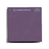
MC68040FE33A Freescale Semiconductor, MC68040FE33A Datasheet - Page 85

MC68040FE33A
Manufacturer Part Number
MC68040FE33A
Description
IC MICROPROCESSOR 32BIT 184-CQFP
Manufacturer
Freescale Semiconductor
Datasheet
1.MC68EC040FE33A.pdf
(442 pages)
Specifications of MC68040FE33A
Processor Type
M680x0 32-Bit
Speed
33MHz
Voltage
5V
Mounting Type
Surface Mount
Package / Case
184-CQFP
Package
184CQFP
Processor Series
M680xx
Core
CPU32
Lead Free Status / RoHS Status
Lead free / RoHS Compliant
Features
-
Lead Free Status / Rohs Status
Details
Available stocks
Company
Part Number
Manufacturer
Quantity
Price
Company:
Part Number:
MC68040FE33A
Manufacturer:
Freescale Semiconductor
Quantity:
10 000
- Current page: 85 of 442
- Download datasheet (4Mb)
SECTION 4
INSTRUCTION AND DATA CACHES
The M68040 contains two independent, 4-Kbyte, on-chip caches located in the physical
address space. Accessing instruction words and data simultaneously through separate
caches increases instruction throughput. The M68040 caches improve system
performance by providing cached data to the on-chip execution unit with very low latency.
Systems with an alternate bus master receive increased bus availability.
Figure 4-1 illustrates the instruction and data caches contained in the instruction and data
memory units. The appropriate memory unit independently services instruction prefetch
and data requests from the integer unit (IU). The memory units translate the logical
address in parallel with indexing into the cache. If the translated address matches one of
the cache entries, the access hits in the cache. For a read operation, the memory unit
supplies the data to the IU, and for a write operation, the memory unit updates the cache.
If the access does not match one of the cache entries (misses in the cache) or a write
access must be written through to memory, the memory unit sends an external bus
request to the bus controller. The bus controller then reads or writes the required data.
Cache coherency in the M68040 is optimized for multimaster applications in which the
M68040 is the caching master sharing memory with one or more noncaching masters
(such as DMA controllers). The M68040 implements a bus snooper that maintains cache
coherency by monitoring an alternate bus master’s access and performing cache
maintenance operations as requested by the alternate bus master. Matching cache entries
can be invalidated during the alternate bus master’s access to memory, or memory can be
inhibited to allow the M68040 to respond to the access as a slave. For an external write
operation, the processor can intervene in the access and update its internal caches (sink
data). For an external read operation, the processor supplies cached data to the alternate
bus muster (source data). This prevents the M68040 caches from accumulating old or
invalid copies of data (stale data). Alternate bus masters are allowed access to locally
modified data within the caches that is no longer consistent with external memory (dirty
data). Allowing memory pages to be specified as write-through instead of copyback also
supports cache coherency. When a processor writes to write-through pages, external
MOTOROLA
Ignore all references to the memory management unit (MMU)
when reading for the MC68EC040 and MC68EC040V. The
functionality of the MC68040 transparent translation registers
has been changed in the MC68EC040 and MC68EC040V to
the access control registers. Refer to Appendix B
MC68EC040 for details.
Freescale Semiconductor, Inc.
For More Information On This Product,
Go to: www.freescale.com
M68040 USER’S MANUAL
NOTE
4- 1
Related parts for MC68040FE33A
Image
Part Number
Description
Manufacturer
Datasheet
Request
R

Part Number:
Description:
(MC600 Series) INTEGRATED CIRCUITS
Manufacturer:
ETC
Datasheet:
Part Number:
Description:
Manufacturer:
Freescale Semiconductor, Inc
Datasheet:
Part Number:
Description:
Manufacturer:
Freescale Semiconductor, Inc
Datasheet:
Part Number:
Description:
Manufacturer:
Freescale Semiconductor, Inc
Datasheet:
Part Number:
Description:
Manufacturer:
Freescale Semiconductor, Inc
Datasheet:
Part Number:
Description:
Manufacturer:
Freescale Semiconductor, Inc
Datasheet:
Part Number:
Description:
Manufacturer:
Freescale Semiconductor, Inc
Datasheet:
Part Number:
Description:
Manufacturer:
Freescale Semiconductor, Inc
Datasheet:
Part Number:
Description:
Manufacturer:
Freescale Semiconductor, Inc
Datasheet:
Part Number:
Description:
Manufacturer:
Freescale Semiconductor, Inc
Datasheet:
Part Number:
Description:
Manufacturer:
Freescale Semiconductor, Inc
Datasheet:
Part Number:
Description:
Manufacturer:
Freescale Semiconductor, Inc
Datasheet:
Part Number:
Description:
Manufacturer:
Freescale Semiconductor, Inc
Datasheet:
Part Number:
Description:
Manufacturer:
Freescale Semiconductor, Inc
Datasheet:
Part Number:
Description:
Manufacturer:
Freescale Semiconductor, Inc
Datasheet:


