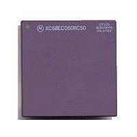
MC68040FE33A Freescale Semiconductor, MC68040FE33A Datasheet - Page 87

MC68040FE33A
Manufacturer Part Number
MC68040FE33A
Description
IC MICROPROCESSOR 32BIT 184-CQFP
Manufacturer
Freescale Semiconductor
Datasheet
1.MC68EC040FE33A.pdf
(442 pages)
Specifications of MC68040FE33A
Processor Type
M680x0 32-Bit
Speed
33MHz
Voltage
5V
Mounting Type
Surface Mount
Package / Case
184-CQFP
Package
184CQFP
Processor Series
M680xx
Core
CPU32
Lead Free Status / RoHS Status
Lead free / RoHS Compliant
Features
-
Lead Free Status / Rohs Status
Details
Available stocks
Company
Part Number
Manufacturer
Quantity
Price
Company:
Part Number:
MC68040FE33A
Manufacturer:
Freescale Semiconductor
Quantity:
10 000
- Current page: 87 of 442
- Download datasheet (4Mb)
Freescale Semiconductor, Inc.
TAG
V
LW3
LW2
LW1
LW0
(a) Instruction Cache Line
TAG
V
LW3
D3
LW2
D2
LW1
D1
LW0
D0
TAG — 22-Bit Physical Address Tag
V — Line VALID Bit
LW — Long Word n (32-Bit) Data Entry
Dn — DIRTY Bit for Long Word n
(b) Data Cache Line
Figure 4-2. Cache Line Formats
The cache stores an entire line, providing validity on a line-by-line basis. Only burst mode
accesses that successfully read four long words can be cached. Memory devices unable
to support bursting can respond to a cache line read or write access by asserting the
transfer burst inhibit (TBI) signal, forcing the processor to complete the access as a
sequence of three long-word accesses. The cache recognizes burst accesses as if the
access were never inhibited, detecting no difference.
A cache line is always in one of three states: invalid, valid, or dirty. For invalid lines, the V-
bit is clear, causing the cache line to be ignored during lookups. Valid lines have their V-bit
set and D-bits cleared, indicating all four long words in the line contain valid data
consistent with memory. Dirty cache lines have the V-bit and one or more D-bits set,
indicating that the line has valid long-word entries that have not been written to memory
(long words whose D-bit is set). A cache line changes from valid to invalid if the execution
of the CINV or CPUSH instruction explicitly invalidates the cache line; if a snooped write
access hits the cache line and the line is not dirty; or if the SCx signals for a snooped read
access invalidates the line. Both caches should be explicitly cleared after a hardware reset
of the processor since reset does not invalidate the cache lines.
Figure 4-3 illustrates the general flow of a caching operation. The corresponding memory
unit translates the logical address of each access to a physical address allowing the IU to
access the data in the cache. To minimize latency of the requested data, the lower
untranslated bits of the logical address map directly to the physical address bits and are
used to access a set of cache lines in parallel with the translation. Physical address bits
9–4 are used to index into the cache and select one of the 64 sets of four cache lines. The
four tags from the selected cache set are compared with the translated physical address
bits 31–12 and bits 11 and 10 of the untranslated page offset. If any one of the four tags
matches and the tag status is either valid or dirty, then the cache has a hit. During read
accesses, a half-line (two long words) is accessed at a time, requiring two cache accesses
for reads that are greater than a half-line or two long words. Write accesses within a cache
line require a single cache access. If a misaligned access crosses two pages, then the
partial access to the first page always happens twice, even if the pages are serialized.
Consequently, if the accesses span page boundaries, misaligned accesses to peripherals
are not possible unless the peripheral can tolerate double reads or writes.
MOTOROLA
M68040 USER’S MANUAL
4- 3
For More Information On This Product,
Go to: www.freescale.com
Related parts for MC68040FE33A
Image
Part Number
Description
Manufacturer
Datasheet
Request
R

Part Number:
Description:
(MC600 Series) INTEGRATED CIRCUITS
Manufacturer:
ETC
Datasheet:
Part Number:
Description:
Manufacturer:
Freescale Semiconductor, Inc
Datasheet:
Part Number:
Description:
Manufacturer:
Freescale Semiconductor, Inc
Datasheet:
Part Number:
Description:
Manufacturer:
Freescale Semiconductor, Inc
Datasheet:
Part Number:
Description:
Manufacturer:
Freescale Semiconductor, Inc
Datasheet:
Part Number:
Description:
Manufacturer:
Freescale Semiconductor, Inc
Datasheet:
Part Number:
Description:
Manufacturer:
Freescale Semiconductor, Inc
Datasheet:
Part Number:
Description:
Manufacturer:
Freescale Semiconductor, Inc
Datasheet:
Part Number:
Description:
Manufacturer:
Freescale Semiconductor, Inc
Datasheet:
Part Number:
Description:
Manufacturer:
Freescale Semiconductor, Inc
Datasheet:
Part Number:
Description:
Manufacturer:
Freescale Semiconductor, Inc
Datasheet:
Part Number:
Description:
Manufacturer:
Freescale Semiconductor, Inc
Datasheet:
Part Number:
Description:
Manufacturer:
Freescale Semiconductor, Inc
Datasheet:
Part Number:
Description:
Manufacturer:
Freescale Semiconductor, Inc
Datasheet:
Part Number:
Description:
Manufacturer:
Freescale Semiconductor, Inc
Datasheet:


