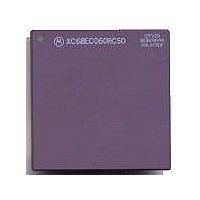
MC68040FE33A Freescale Semiconductor, MC68040FE33A Datasheet - Page 89

MC68040FE33A
Manufacturer Part Number
MC68040FE33A
Description
IC MICROPROCESSOR 32BIT 184-CQFP
Manufacturer
Freescale Semiconductor
Datasheet
1.MC68EC040FE33A.pdf
(442 pages)
Specifications of MC68040FE33A
Processor Type
M680x0 32-Bit
Speed
33MHz
Voltage
5V
Mounting Type
Surface Mount
Package / Case
184-CQFP
Package
184CQFP
Processor Series
M680xx
Core
CPU32
Lead Free Status / RoHS Status
Lead free / RoHS Compliant
Features
-
Lead Free Status / Rohs Status
Details
Available stocks
Company
Part Number
Manufacturer
Quantity
Price
Company:
Part Number:
MC68040FE33A
Manufacturer:
Freescale Semiconductor
Quantity:
10 000
- Current page: 89 of 442
- Download datasheet (4Mb)
Freescale Semiconductor, Inc.
4.2 CACHE MANAGEMENT
Using the MOVEC instruction, the caches are individually enabled to access the 32-bit
cache control register (CACR) illustrated in Figure 4-4. The CACR contains two enable
bits that allow the instruction and data caches to be independently enabled or disabled.
Setting one of these bits enables the associated cache without affecting the state of any
lines within the cache. A hardware reset clears the CACR, disabling both caches;
however, reset does not affect the tags, state information, and data within the caches. The
CINV instruction must clear the caches before enabling them. It is not recommended that
page descriptors be cached. Specifically, the M68040 does not support the caching of
page descriptors in copyback mode with the bit pattern U = 0, M = 1, and R = 1 in a page
descriptor. The M68040 table search algorithm will never leave this bit pattern for a page
descriptor.
31
30
16
15
14
0
DE
UNDEFINED
IE
UNDEFINED
DE = Enable Data Cache
IE = Enable Instruction Cache
Figure 4-4. Cache Control Register
System hardware can assert the cache disable (CDIS) signal to dynamically disable both
caches, regardless of the state of the enable bits in the CACR. The caches are disabled
immediately after the current access completes. If CDIS is asserted during the access for
the first half of a misaligned operand spanning two cache lines, the data cache is disabled
for the second half of the operand. Accesses by the execution units bypass the caches
while they are disabled and do not affect their contents (with the exception of CINV and
CPUSH instructions). Disabling the caches with CDIS does not affect snoop operations.
CDIS is intended primarily for use by in-circuit emulators to allow swapping between the
tags and emulator memories.
Even if the instruction cache is disabled, the M68040 can cache instructions because of
an internal cache line register. This happens for instruction loops that are completely
resident within the first six bytes of a half-line. Thus, the cache line holding register can
operate as a small cache. If a loop fits anywhere within the first three words of a half-line,
then it becomes cached.
The CINV and CPUSH instructions support cache management in the supervisor mode.
CINV allows selective invalidation of cache entries. CPUSH performs two operations: 1)
any selected data cache lines containing dirty data are pushed to memory; 2) all selected
cache lines are invalidated. This operation can be used to update a page in memory
before swapping it out with snooping disabled or to push dirty data when changing a page
caching mode to write-through. Because of the size of the caches, pushing pages or an
entire cache incurs a significant time penalty. However, these instructions are
interruptable to avoid large interrupt latencies. The state of the CDIS signal or the cache
enable bits in the CACR does not affect the operation of CINV and CPUSH. Both
instructions allow operation on a single cache line, all cache lines in a specific page, or an
MOTOROLA
M68040 USER’S MANUAL
4- 5
For More Information On This Product,
Go to: www.freescale.com
Related parts for MC68040FE33A
Image
Part Number
Description
Manufacturer
Datasheet
Request
R

Part Number:
Description:
(MC600 Series) INTEGRATED CIRCUITS
Manufacturer:
ETC
Datasheet:
Part Number:
Description:
Manufacturer:
Freescale Semiconductor, Inc
Datasheet:
Part Number:
Description:
Manufacturer:
Freescale Semiconductor, Inc
Datasheet:
Part Number:
Description:
Manufacturer:
Freescale Semiconductor, Inc
Datasheet:
Part Number:
Description:
Manufacturer:
Freescale Semiconductor, Inc
Datasheet:
Part Number:
Description:
Manufacturer:
Freescale Semiconductor, Inc
Datasheet:
Part Number:
Description:
Manufacturer:
Freescale Semiconductor, Inc
Datasheet:
Part Number:
Description:
Manufacturer:
Freescale Semiconductor, Inc
Datasheet:
Part Number:
Description:
Manufacturer:
Freescale Semiconductor, Inc
Datasheet:
Part Number:
Description:
Manufacturer:
Freescale Semiconductor, Inc
Datasheet:
Part Number:
Description:
Manufacturer:
Freescale Semiconductor, Inc
Datasheet:
Part Number:
Description:
Manufacturer:
Freescale Semiconductor, Inc
Datasheet:
Part Number:
Description:
Manufacturer:
Freescale Semiconductor, Inc
Datasheet:
Part Number:
Description:
Manufacturer:
Freescale Semiconductor, Inc
Datasheet:
Part Number:
Description:
Manufacturer:
Freescale Semiconductor, Inc
Datasheet:


