MCR106-3 ON Semiconductor, MCR106-3 Datasheet
MCR106-3
Specifications of MCR106-3


Related parts for MCR106-3


MCR106-3 Summary of contents
Page 1
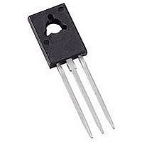
... MCR106-6, MCR106-8 Preferred Device Sensitive Gate Silicon Controlled Rectifiers Reverse Blocking Thyristors PNPN devices designed for high volume consumer applications such as temperature, light and speed control; process and remote control, and warning systems where reliability of operation is important. Features Glass-Passivated Surface for Reliability and Uniformity ...
Page 2
... DYNAMIC CHARACTERISTICS Critical Rate−of−Rise of Off−State Voltage (T = 110 kW Pulse Test: Pulse Width 1.0 ms, Duty Cycle 4. R current is not included in measurement. GK ORDERING INFORMATION Device MCR106−6 MCR106−6G MCR106−8 MCR106− unless otherwise noted 110 kW) GK 1%. Package TO−225AA TO−225AA (Pb−Free) TO− ...
Page 3
Voltage Current Characteristic of SCR Symbol Parameter V Peak Repetitive Off State Forward Voltage DRM I Peak Forward Blocking Current DRM V Peak Repetitive Off State Reverse Voltage RRM I Peak Reverse Blocking Current RRM V Peak On State Voltage ...
Page 4
... TYP Q 0.148 0.158 3.76 4.01 R 0.045 0.065 1.15 1.65 S 0.025 0.035 0.64 0.88 U 0.145 0.155 3.69 3.93 V 0.040 --- 1.02 --- STYLE 2: PIN 1. CATHODE 2. ANODE 3. GATE ON Semiconductor Website: www.onsemi.com Order Literature: http://www.onsemi.com/orderlit For additional information, please contact your local Sales Representative MCR106/D ...