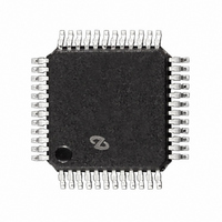
LM98501CCVBH National Semiconductor, LM98501CCVBH Datasheet - Page 14

LM98501CCVBH
Manufacturer Part Number
LM98501CCVBH
Description
IC CAMERA SIGNAL PROCESS 48-LQFP
Manufacturer
National Semiconductor
Type
Camera Interfacer
Datasheet
1.LM98501CCVBH.pdf
(24 pages)
Specifications of LM98501CCVBH
Applications
Digital Camera, Conferencing, Scanner
Mounting Type
Surface Mount
Package / Case
48-LQFP
Lead Free Status / RoHS Status
Contains lead / RoHS non-compliant
Other names
*LM98501CCVBH
www.national.com
System Overview
PROGRAMMABLE GAIN AMPLIFIER
In a CCD imager, there may be millions of photo diodes that
normally have some gain variation from pixel to pixel. Other
gain errors are generated by the amount of light transmis-
sion and the quality of the color filters on the front of each
pixel of the imager. These filters make it possible for camera
to recognize color; therefore, each filter has to have correct
gain in order to generate the electronic voltages that would
be equal to white. Luminosity of a scene may have a color-
cast, and the gain of a pixel must be changed in order to
compensate for the colorcast. These three sources of gain
error associated with each pixel are compensated for with a
wide bandwidth programmable gain amplifier that operates
at a pixel rate. The amplifier has a gain ranging from
0 dB–32 dB, and is “linear in dB” as shown in Figure 16 . A
linear in dB amplifier contains more gain steps in the lower
portion of the gain range so that color balance may be main-
tained during low light levels.
AUXILIARY INPUT
The LM98501 includes a high-level video switch that allows
a recorder playback video signal to be selected instead of
the camera image. This feature is especially useful when
adding electronic titles to images in the digital domain. In ad-
dition, the PGA gain and DAC offset are set to register 0 in
FIGURE 9. Correlated Double Sampling
(Continued)
FIGURE 10. Digital Black Level Correction Loop
DS101292-10
14
each case; therefore, appropriate gain and offset values
should be written to PGA gain and DAC offset register 0 prior
AUX IN usage.
BLACK LEVEL CLAMP
CCD signal processors require a reference level for the
proper handling of input signals; this reference level is com-
monly referred to as the black level. The LM98501 is de-
signed to determine a signal’s black level during the CCD im-
ager’s optical black pixels.
The LM98501 provides both an analog clamp and a digital
black level correction loop. Pulsing the ACLP pin during op-
tical black pixels causes the analog clamp circuitry to re-
move the offset associated with the input signal. During
dummy black pixels at the end of a horizontal line, setting the
BLKCLP pin for a minimum of 20 CLK cycles enables the
digital black level correction loop.
Actual black level correction may be performed through one
of two available methods — automatic or manual. In auto-
matic mode, the black level is sampled from the ADC output
during black pixels by setting the BLKCLP input of the
LM98501. The ADC black level output value is then aver-
aged over eight pixels and subtracted from the desired black
level stored in the black level configuration register. The re-
sult of the subtraction may then be integrated by a preset
scaling factor, effectively smoothing any sharp transitions
present in the black level signal, before the resulting error is
finally applied to the input of the PGA as an analog offset
generated by the DAC. The offset integration scaling factor is
stored in two bits of the software control register 0, and the
values available range from the full offset to offset
divided-by-16. In addition, an offset output enable bit is pro-
vided in the software control register 0, which when set,
routes the offset value to the digital output bus rather than
the DAC. Use of the automatic mode involves enabling the
black level offset auto-calibration bit in the software control
register 0 through the serial interface.
The manual method is intended for use with processing sys-
tems where the desired black level correction loop is exter-
nal to the LM98501. In this mode, up to four available con-
figuration registers may be used to store predetermined
offset values that will be applied on a pixel-rate basis. During
the vertical interval, new values may be stored in these reg-
isters for each horizontal line.
DS101292-11


