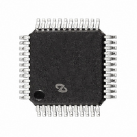
LM98501CCVBH National Semiconductor, LM98501CCVBH Datasheet - Page 4

LM98501CCVBH
Manufacturer Part Number
LM98501CCVBH
Description
IC CAMERA SIGNAL PROCESS 48-LQFP
Manufacturer
National Semiconductor
Type
Camera Interfacer
Datasheet
1.LM98501CCVBH.pdf
(24 pages)
Specifications of LM98501CCVBH
Applications
Digital Camera, Conferencing, Scanner
Mounting Type
Surface Mount
Package / Case
48-LQFP
Lead Free Status / RoHS Status
Contains lead / RoHS non-compliant
Other names
*LM98501CCVBH
www.national.com
Pin
11
12
13
14
15
16
17
18
19
20
21
22
23
24
25
26
27
28
29
30
31
32
33
34
35
36
37
38
39
40
41
42
43
44
45
Pin Descriptions
Name
DV+
CLK
SHP
SHD
BOL
BLKCLP
V
V
V
CE
SCLK
SI DATA
SO DATA
DGND I/O
DV+ I/O
D0
D1
D2
D3
D4
D5
D6
D7
D8
D9
DV+ I/O
DGND I/O
DGND
DV+
AV+
AGND
V
AV+
AGND
AOUT−
REFP
REFN
REFB
REFT
I/O
IO
IO
IO
IO
O
O
O
O
O
O
O
O
O
O
O
O
I
I
I
I
I
I
I
I
(Continued)
Typ
D
D
D
D
D
D
D
D
D
D
D
D
D
D
D
D
D
D
D
P
A
A
A
P
P
P
P
P
P
P
P
A
P
P
A
+3V power supply for the digital circuits. Bypass each supply pin with 0.1 µF and
10 µF capacitors in parallel.
27 MHz clock input.
Correlated double sampler reset voltage clamp override. Programmable active-high or
active-low through serial interface. Connect to +3V digital supply when function not
being used (register values in default condition).
Correlated double sampler video signal voltage sample override. Programmable
active-high or active-low through serial interface. Connect to +3V digital supply when
function not being used (register values in default condition).
Active-high beginning of line switch input. Hold high during entire line of effective
pixels. Hold low during blanking period.
Active-high black level clamp switch input. Pulse high during black pixels to eliminate
black pixel offset from video signal.
Top of DAC reference ladder. Normally bypassed with a 0.1 µF capacitor. An external
DAC reference voltage may be applied to this pin.
Bottom of DAC reference ladder. Normally bypassed with a 0.1 µF capacitor. An
external DAC reference voltage may be applied to this pin.
Bottom of ADC reference ladder. Normally bypassed with a 0.1 µF capacitor. An
external ADC reference voltage may be applied to this pin.
Active-low chip enable for the serial interface.
Serial interface clock used to decode the serial input data.
Serial interface input port.
Serial interface output port.
Digital output driver ground return.
+3V power supply for the digital output driver circuits. Bypass each supply pin with
0.1 µF and 10 µF capacitors in parallel.
Digital output. Bit 0 of 9 (LSB) of the digital video output bus.
Digital output. Bit 1 of 9 of the digital video output bus.
Digital output. Bit 2 of 9 of the digital video output bus.
Digital output. Bit 3 of 9 of the digital video output bus.
Digital output. Bit 4 of 9 of the digital video output bus.
Digital output. Bit 5 of 9 of the digital video output bus.
Digital output. Bit 6 of 9 of the digital video output bus.
Digital output. Bit 7 of 9 of the digital video output bus.
Digital output. Bit 8 of 9 of the digital video output bus.
Digital output. Bit 9 of 9 (MSB) of the digital video output bus.
+3V power supply for the digital output driver circuits. Bypass each supply pin with
0.1 µF and 10 µF capacitors in parallel.
Digital output driver ground return.
Digital ground return.
+3V power supply for the digital circuits. Bypass each supply pin with 0.1 µF and 10
µF capacitors in parallel.
+3V power supply for the analog circuits. Bypass each supply pin with 0.1 µF and 10
µF capacitors in parallel.
Analog ground return.
Top of ADC reference ladder. Normally bypassed with a 0.1 µF capacitor. An external
ADC reference voltage may be applied to this pin.
+3V power supply for the analog circuits. Bypass each supply pin with 0.1 µF and 10
µF capacitors in parallel.
Analog ground return.
Negative differential analog output from correlated double sampler or PGA (selectable
through the serial interface).
4
Description


