DS2505 Maxim Integrated Products, DS2505 Datasheet
DS2505
Specifications of DS2505
Available stocks


Related parts for DS2505

DS2505 Summary of contents
Page 1
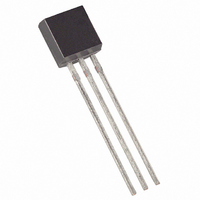
... For details see the Package Information section. ORDERING INFORMATION specifies DS2505 DS2505 DS2505/T&R DS2505P DS2505P/T&R TSOC Package, Tape & Reel DS2505+ DS2505+T&R DS2505P+ DS2505P+T&R TSOC Package, Tape & Reel + Denotes a lead(Pb)-free/RoHS-compliant package 16Kb Add-Only Memory TSOC PACKAGE TO-92 1 DALLAS GND DS2505 2 ...
Page 2
... LASERED ROM Each DS2505 contains a unique ROM code that is 64 bits long. The first 8 bits are a 1-Wire family code. The next 48 bits are a unique serial number. The last 8 bits are a CRC of the first 56 bits. (See Figure 3.) The 64-bit ROM and ROM Function Control section allow the DS2505 to operate as a 1-Wire device and follow the 1-Wire protocol detailed in the section “ ...
Page 3
... After the 8th bit of the family code has been entered, then the serial number is entered. After the 48 has been entered, the shift register contains the CRC value. Shifting in the 8 bits of CRC should return the shift register to all zeroes. DS2505 BLOCK DIAGRAM Figure ...
Page 4
... MSB 16384-BITS EPROM The memory map in Figure 4 shows the 16384-bit EPROM section of the DS2505 which is configured as 64 pages of 32 bytes each. The 8-bit scratchpad is an additional register that acts as a buffer when programming the memory. Data is first written to the scratchpad and then verified by reading a 16-bit CRC from the DS2505 that confirms proper receipt of the data and address ...
Page 5
... EPROM STATUS BYTES In addition to the 16384 bits of data memory the DS2505 provides 704 bits of Status Memory accessible with separate commands. The EPROM Status Bytes can be read or programmed to indicate various conditions to the software interrogating the DS2505. The first 8 bytes of the EPROM Status Memory (addresses 000 to 007H) contain the Write Protect Page bits which inhibit programming of the corresponding page in the 16384-bit main memory area if the appropriate write protection bit is programmed ...
Page 6
... The Status Memory address range of the DS2505 extends from 000 to 13FH. The memory locations 008H to 01FH, 028H to 03FH, 048H to 0FFH and 140H to 7FFH are physically not implemented. Reading these locations will usually result in FFH bytes. Attempts to write to these locations will be ignored. If the bus master sends a starting address higher than 7FFH, the five most significant address bits are set the internal circuitry of the chip ...
Page 7
... With every subsequent read data time slot the bus master receives data from the DS2505 starting at the supplied address and continuing until the end of an 8-byte page of the EPROM Status data field is reached. At that point the bus master will receive a 16-bit CRC of the command byte, address bytes and status data bytes ...
Page 8
... MEMORY FUNCTION FLOW CHART Figure ...
Page 9
... MEMORY FUNCTION FLOW CHART Figure 5 (cont’ ...
Page 10
... MEMORY FUNCTION FLOW CHART Figure 5 (cont’ ...
Page 11
... EPROM Status data field. After the 16-bit CRC of the last EPROM Status data page is read, the bus master will receive logical 1s from the DS2505 until a reset pulse is issued. The Read Status command sequence can be ended at any point by issuing a reset pulse. ...
Page 12
... CRC that is the result of clearing the CRC generator and then shifting in the Redirection Byte only. After the 16-bit CRC of the last page is read, the bus master will receive logical 1s from the DS2505 until a Reset Pulse is issued. The Extended Read Memory command sequence can be exited at any point by issuing a Reset Pulse ...
Page 13
... As the DS2505 receives this byte of data into the scratchpad, it also shifts the data into the CRC generator that has been preloaded with the current address and the result is a 16-bit CRC of the new data byte and the new address. After supplying the data byte, the bus master will read this 16-bit CRC from the DS2505 with sixteen read time slots to confirm that the address incremented properly and the data byte was received correctly ...
Page 14
... As the DS2505 receives this byte of data into the scratchpad, it also shifts the data into the CRC generator that has been preloaded with the current address and the result is a 16-bit CRC of the new data byte and the new address ...
Page 15
... The presence pulse lets the bus master know that the DS2505 is on the bus and is ready to operate. For more details, see the “1-Wire Signaling” section. ...
Page 16
... DS2505 EQUIVALENT CIRCUIT Figure 6 BUS MASTER CIRCUIT Figure ...
Page 17
ROM FUNCTIONS FLOW CHART Figure ...
Page 18
... DS2505. During write time slots, the delay circuit determines when the DS2505 will sample the data line. For a read data time slot “0” transmitted, the delay circuit determines how long the DS2505 will hold the data line low overriding the 1 generated by the master. If the data bit is a “ ...
Page 19
... Note that due to the high voltage programming requirements for any 1-Wire EPROM device not possible to multidrop non-EPROM based 1-Wire devices with the DS2505 during programming. An internal diode within the non-EPROM based 1-Wire devices will attempt to clamp the data line at approximately 8 volts and could potentially damage these devices. ...
Page 20
READ/WRITE TIMING DIAGRAM Figure 10 (cont’d) NOTE: For read-data time slots the optimal sampling point for the master is as close as possible to the end of the t period without exceeding the 15 µs window. For the case of ...
Page 21
... ROM. The bus master can compute a CRC value from the first 56 bits of the 64-bit ROM and compare it to the value stored within the DS2505 to determine if the ROM data has been received error-free by the bus master. The equivalent polynomial ...
Page 22
... There is no circuitry on the DS2505 that prevents a command sequence from proceeding if the CRC stored in or calculated by the DS2505 does not match the value generated by the bus master. For more details on generating CRC values including example implementations in both hardware and software, see the Book of DS19xx iButton Standards ...
Page 23
ABSOLUTE MAXIMUM RATINGS* Voltage on any Pin Relative to Ground Operating Temperature Storage Temperature Soldering Temperature * This is a stress rating only and functional operation of the device at these or any other conditions outside those indicated in the ...
Page 24
... If V PUP may not reproduce the correct memory contents. Therefore, under low voltage conditions recommended to set either the most significant bit or all five most significant bits of TA2 to 1. Internal circuitry of the chip will force these 5 bits back to 0 before they are shifted in the address counter and CRC generator ...