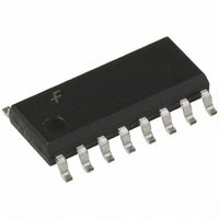
FAN5067MX Fairchild Semiconductor, FAN5067MX Datasheet - Page 10

FAN5067MX
Manufacturer Part Number
FAN5067MX
Description
IC CTRLR SW ACPI DUAL 16SOIC
Manufacturer
Fairchild Semiconductor
Datasheet
1.FAN5067M.pdf
(14 pages)
Specifications of FAN5067MX
Applications
Controller, Intel Pentium® IV
Number Of Outputs
2
Voltage - Output
3.3V, 5V, Adjustable
Operating Temperature
0°C ~ 70°C
Mounting Type
Surface Mount
Package / Case
16-SOIC (3.9mm Width)
Output Voltage
10 V
Operating Temperature Range
0 C to + 70 C
Mounting Style
SMD/SMT
Lead Free Status / RoHS Status
Lead free / RoHS Compliant
Voltage - Input
-
Lead Free Status / Rohs Status
Lead free / RoHS Compliant
FAN5067
Adjustable Dual Output
The adjustable dual output is intended to provide power to
SDRAM or DDR memory.
Adjustable dual is generated by one external NPN bipolar
acting as a linear regulator from +5V main, and one linear
regulator internal to the FAN5067 from +5V standby, as
shown in Figure 4, and in the block diagram on the front
page. When main power is present, the NPN Q3 linear regu-
lates, and when main power is absent, the internal linear reg-
ulator is on. Q3 cannot be substituted with a MOSFET. If
used in one direction, the MOSFET’s body diode would per-
mit back-feed; if used in the other direction, it would short-
circuit the linear regulator action.
The state of the external MOSFET and the internal linear
regulator is controlled by the SLP_S3 and PWROK lines,
and additionally the SLP_S5 line, as shown in Figure 3.
When SLP_S5 is de-asserted, both the external MOSFET
and the internal linear regulator are off, and there is no out-
put voltage on the 3.3V SDRAM line.
If the SLP_S5 line is asserted, the adjustable dual output is
on. In this condition, if either the SLP_S3 or the PWROK
line, or both, are de-asserted, the linear regulator is on and
the MOSFET is off. Only in the case if both the SLP_S3 and
the PWROK lines are asserted, the MOSFET is on and the
linear regulator is off.
In a typical system, it is anticipated that standby current will
be a maximum of 365mA, and full-power current may be as
high as 2A. This places some significant constraints on the
selection of Q3. Since its input may be as low as (5V – 5%)
= 4.75V, there is only 4.75V – 3.3V = 1.45mV of V
room for its operation as a linear regulator. For this reason
the FAN5067 can provide up to 200mA of steady-state base
current. The TIP41A device shown has a sufficiently low
V
this base current.
10
ESR (m )
CE, sat
to guarantee worst-case regulation even at 2A I
Figure 6. Recommended C vs. ESR for
300
200
100
Stable Operation of the Dual Output
47
100
C ( F)
200
300
330
400
CE
E
with
head-
The output voltage of the Adjustable Dual is set with two
resistors as shown in Figure 4, according to the equation.
Dynamic Change of Adjust Output
There may be circumstances under which it is desired to
dynamically change the output of the adjustable dual output.
For example, a circuit that switches from 2.5V to 3.3V is
shown in Figure 7.
A potential problem arises when using this circuit, however:
When the transistor is turned on, the voltage on the VADJFB
pin abruptly drops, until the output of the linear regulator can
charge up the output caps. If the voltage to which it drops is
less than about 80% of 1.25V, or 1.00V, the OC limit will trip
and shut down the IC. This happens in this example because
To avoide this problem, systems that intended to dynami-
cally change the output voltage of the adjustable dual output
should disable the OC protection with the circuit shown in
Figure 8.
Figure 7. Circuit for Dynamic Change of Output Voltage
Figure 8. Circuit to Disable OC Protection
SS
2.5V
VADJFB
Vadj
VADJ
3.3V
-----------------------------------------
of the Adjustable
R
C
=
2
SS
R
1.25V
2
R
2N3906
3
R
+5V_SB
+
3
1N4148
R1
PRODUCT SPECIFICATION
R
------------------ -
1
R
+
=
+
2
R
0.94V
2
500K
1 F
REV. 1.0.1 5/2/02


