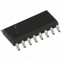
FAN5067MX Fairchild Semiconductor, FAN5067MX Datasheet - Page 12

FAN5067MX
Manufacturer Part Number
FAN5067MX
Description
IC CTRLR SW ACPI DUAL 16SOIC
Manufacturer
Fairchild Semiconductor
Datasheet
1.FAN5067M.pdf
(14 pages)
Specifications of FAN5067MX
Applications
Controller, Intel Pentium® IV
Number Of Outputs
2
Voltage - Output
3.3V, 5V, Adjustable
Operating Temperature
0°C ~ 70°C
Mounting Type
Surface Mount
Package / Case
16-SOIC (3.9mm Width)
Output Voltage
10 V
Operating Temperature Range
0 C to + 70 C
Mounting Style
SMD/SMT
Lead Free Status / RoHS Status
Lead free / RoHS Compliant
Voltage - Input
-
Lead Free Status / Rohs Status
Lead free / RoHS Compliant
FAN5067
UVLO
If the +5V standby is below approximately 4.5V, the
FAN5067 will leave off or turn off all outputs. Similar com-
ments apply to the +12V main at 7.5V. The +5V standby
UVLO has approximately 0.5V hysteresis, the +12V main
UVLO 1V.
Over Temperature
The FAN5067 is capable of sourcing substantial current,
200mA minimum to the adjustable voltage transistor’s base dur-
ing S0 and 144mA to the line during S3. As a result, there can
be heavy power dissipation in the IC. While the FAN5067 is
designed to accept this power dissipation, any overloading of
outputs can cause excessive heating. If the FAN5067 die
temperature exceeds about 150°, all outputs are shut off.
Outputs remain off until the die temperature returns to its
safe area.
Transistor Selection
External transistor selection depends on usage, differing for
the linear regulators and the switches.
The MOSFET switches, should be sized based on regulation
requirements and power dissipation. Since the ATX outputs
are ±5%, the outputs driven from them must be wider. As an
example, if we want to hold 3.3V PCI to -10%, we can drop
only 5% = 165mV across Q1. At 2.4A, this means Ql must
have a maximum R
tolerance and self-heating effects. We thus choose a Fairchild
FDC633N, which has 72m maximum R
at 25°C. We can estimate power dissipation as (2.4A)
42m = 270mW, which should be acceptable for this pack-
age.
Q2 is a MOSFET functioning as a linear regulator. Since it
delivers only 500mA, it is easy to select a MOSFET, it need
only be able to handle 500mA * (5V + 5% – 3.3V) = 1W.
We select the Fairchild FDS6630A in an SO-8 package.
Q3 is an NPN bipolar functioning as a linear regulator. As
already discussed, it must have a V
I
high as (5V + 5%–3.3V) * 2A = 3.9W.
Alternate for Adjustable Dual
Instead of the bipolar transistor shown in Figure 4 for Q3, the
linear pass element for the adjustable dual, a MOSFET and
schottky diode can be used as shown in Figure 9.
12
E
= 2A and I
B
= 200mA. Its power dissipation can be as
DS,on
of 165mV/2.7A = 68m , including
CE,sat
lower than 1.45V at
DS, on
at 4.5V V
2
*
GS
The schottky should be chosen to have a low V
fied adjustable voltage and current. The MOSFET’s R
must then be lower than (5V -5% -VADJ -V
temperature. An additional constraint is that the MOSFET
must have a gate threshold voltage lower than 1.5V. For exam-
ple, for 2.8A @3.3V, choose the diode to be an MBR835, and
the MOSFET a Fairchild FDC653M. This same technique
can then also be used for adjustable currents higher than can
be achieved with the bipolar transistor.
Output Capacitor Selection
Output capacitor selection depends on whether the line has
overlap time or not.
For both the adjustable dual, there is guaranteed overlap time
between when one source is turned on and the other source
turned off. For this output, the output capacitor is not needed
to hold up the supply, but only for noise filtering and to
respond to transient loading.
The dual output has deadtime between when one source is
turned off and the other source turned on. During the time
when both are off, the output current must be supplied by the
output capacitor. Mitigating this, it must be realized that the
system will be designed in such a way that the current has
gone to its sleep value before the transition occurs. For
example, the dual has a sleep current of 500mA maximum.
Maximum deadtime is 6µsec, and so charge depletion is
500mA * 6µsec = 3µC. Suppose that we have a total of
8% drop due to the source tolerance and the MOSFET drop,
and we are trying to hold 10% regulation. The remaining
2% = 66mV implies a minimum capacitance of 3µC/66m
V = 45µF.
Figure 9. Adjustable Dual with MOSFET
FAN5067 14
12
Adjustable Dual
PRODUCT SPECIFICATION
5V Main
REV. 1.0.1 5/2/02
f
)/I
Dual
f
at the speci-
including
DS,on


