T89C51CC02CA-TDSIM Atmel, T89C51CC02CA-TDSIM Datasheet
T89C51CC02CA-TDSIM
Specifications of T89C51CC02CA-TDSIM


Related parts for T89C51CC02CA-TDSIM


T89C51CC02CA-TDSIM Summary of contents
Page 1
Features • 80C51 Core Architecture • 256 Bytes of On-chip RAM • 256 Bytes of On-chip XRAM • 16K Bytes of On-chip Flash Memory – Data Retention: 10 Years at 85°C – Erase/Write Cycle: 100K • 2K Bytes of On-chip ...
Page 2
Description Block Diagram XTAL1 XTAL2 CPU T89C51CC02 2 TM Part of the CANary family of 8-bit microcontrollers dedicated to CAN network applica- tions, the T89C51CC02 is a low-pin count 8-bit Flash microcontroller Mode a maximum external clock rate ...
Page 3
Pin Configurations 4126F–CAN–12/03 VAREF 28 1 VAGND VAVCC 3 25 P4.1/RxDC 4 P4.0/TxDC P2 P3.7 SO28 8 21 P3.6 9 P3.5/T1 20 P3.4/ P3.3/INT1 P3.2/INT0 17 ...
Page 4
T89C51CC02 4 24 P4.0/TxDC P3.7 3 P3.6 QFP- P3.5/T1 5 P3.4/ P3.3/INT1 8 P1.3/AN3/CEX0 P1.4/AN4/CEX1 P1.5/AN5 P1.6/AN6 P1.7/AN7 P2.0 NC RESET 4126F–CAN–12/03 ...
Page 5
Pin Description Pin Name Type Description VSS GND Circuit ground VCC Supply Voltage VAREF Reference Voltage for ADC (input) VAVCC Supply Voltage for ADC VAGND Reference Ground for ADC (internaly connected with the VSS) P1.0:7 I/O Port ...
Page 6
Pin Name Type Description P3.0:7 I/O Port 8-bit bi-directional I/O port with internal pull-ups. Port 3 pins that have 1’s written to them are pulled high by the internal pull-up transistors and can be used as inputs ...
Page 7
I/O Configurations Port Structure 4126F–CAN–12/03 Each Port SFR operates via type-D latches, as illustrated in Figure 1 for Ports 3 and 4. A CPU ’write to latch’ signal initiates transfer of internal bus data into the type-D latch. A CPU ...
Page 8
Read-Modify-Write Instructions Quasi Bi-directional Port Operation T89C51CC02 8 Some instructions read the latch data rather than the pin data. The latch based instruc- tions read the data, modify the data and then rewrite the latch. These are called ’Read- Modify-Write’ ...
Page 9
This is traditional CMOS switch convention. Current strengths are 1/10 that of pFET #3. Note: During Reset, pFET#1 is not avtivated. During Reset, only the weak pFET#3 pull up the pin. Figure 2. Internal ...
Page 10
SFR Mapping Table 2. C51 Core SFRs Mnemonic Add Name ACC E0h Accumulator B F0h B Register PSW D0h Program Status Word SP 81h Stack Pointer Data Pointer Low byte DPL 82h LSB of DPTR Data Pointer High byte DPH ...
Page 11
Table 4. Timers SFRs (Continued) Mnemonic Add Name Timer/Counter 2 T2CON C8h control Timer/Counter 2 T2MOD C9h Mode Timer/Counter 2 RCAP2H CBh Reload/Capture High byte Timer/Counter 2 RCAP2L CAh Reload/Capture Low byte WatchDog Timer WDTRST A6h Reset WatchDog Timer WDTPRG ...
Page 12
Table 6. PCA SFRs (Continued) Mnemonic Add Name PCA Compare CCAP0L EAh Capture Module 0 L CCAP1L EBh PCA Compare Capture Module 1 L Table 7. Interrupt SFRs Mnemonic Add Name Interrupt Enable IEN0 A8h Control 0 Interrupt Enable IEN1 ...
Page 13
Table 9. CAN SFRs (Continued) Mnemonic Add Name CAN Enable CANEN CFh Channel byte CAN General CANGIE C1h Interrupt Enable CAN Interrupt CANIE C3h Enable Channel byte CAN Status Interrupt CANSIT BBh Channel byte CANTCON A1h CAN Timer Control CANTIMH ...
Page 14
Table 9. CAN SFRs (Continued) Mnemonic Add Name CAN Identifier Mask byte 2(PartA) CANIDM2 C5h CAN Identifier Mask byte 2(PartB) CAN Identifier Mask byte 3(PartA) CANIDM3 C6h CAN Identifier Mask byte 3(PartB) CAN Identifier Mask byte 4(PartA) CANIDM4 C7h CAN ...
Page 15
Table 11. SFR Mapping (1) 0/8 1/9 IPL1 CH F8h xxxx x000 0000 0000 B F0h 0000 0000 IEN1 CL E8h xxxx x000 0000 0000 ACC E0h 0000 0000 CCON CMOD D8h 0000 0000 0xxx x000 PSW FCON D0h 0000 ...
Page 16
Clock Description T89C51CC02 16 The T89C51CC02 core needs only 6 clock periods per machine cycle. This feature, called “X2”, provides the following advantages: • Divides frequency crystals by 2 (cheaper crystals) while keeping the same CPU power. • Saves power ...
Page 17
Figure 3. Clock CPU Generation Diagram Hardware Byte XTAL1 XTAL2 PD PCON CKCON.0 CANX2 CKCON.7 4126F–CAN–12/03 X2B PCON.0 On RESET IDL X2 CKCON ...
Page 18
Figure 4. Mode Switching Waveforms XTAL1 XTAL2 X2 bit CPU clock STD Mode Note order to prevent any incorrect operation while operating in the X2 Mode, users must be aware that all peripherals using the clock frequency as ...
Page 19
Register 4126F–CAN–12/03 Table 12. CKCON Register CKCON (S:8Fh) Clock Control Register CANX2 WDX2 PCAX2 Bit Bit Number Mnemonic Description (1) CAN Clock 7 CANX2 Clear to select 6 clock periods per peripheral clock cycle. Set to select ...
Page 20
Power Management Reset Pin At Power-up (cold reset) T89C51CC02 20 Two power reduction modes are implemented in the T89C51CC02: the Idle mode and the Power-down mode. These modes are detailed in the following sections. In addition to these power reduction ...
Page 21
During a Normal Operation (Warm Reset) Watchdog Reset 4126F–CAN–12/03 Table 14. Minimum Reset Capacitor for a 15k Pull-down Resistor oscrst/vddrst 1ms 5ms 2.7µF 20ms 10µF Note: These values assume VDD starts from 0v to the nominal value. If the time ...
Page 22
Reset Recommendation to Prevent Flash Corruption Idle Mode Entering Idle Mode Exiting Idle Mode Power-down Mode Entering Power-down Mode T89C51CC02 22 When a Flash program memory is embedded on-chip strongly recommended to use an external reset chip (brown ...
Page 23
Exiting Power-down Mode Figure 8. Power-down Exit Waveform Using INT1:0# INT1:0# OSC Active phase 4126F–CAN–12/03 V Note: If was reduced during the Power-down mode, do not exit Power-down mode until restored to the normal operating level. DD ...
Page 24
Registers T89C51CC02 24 Table 15. PCON Register PCON (S:87h) Power Control Register SMOD1 SMOD0 - Bit Bit Number Mnemonic Description Serial port Mode bit 1 7 SMOD1 Set to select double baud rate in mode 1, 2 ...
Page 25
Data Memory Internal Space Lower 128 Bytes RAM 4126F–CAN–12/03 The T89C51CC02 provides data memory access in two different spaces: The internal space mapped in three separate segments: • The lower 128 Bytes RAM segment. • The upper 128 Bytes RAM ...
Page 26
Upper 128 Bytes RAM Expanded RAM T89C51CC02 26 Figure 10. Lower 128 Bytes Internal RAM Organization 30h 20h 18h 10h 08h 00h The upper 128 Bytes of RAM are accessible from address 80h to FFh using only indirect addressing mode. ...
Page 27
Dual Data Pointer Description Application 4126F–CAN–12/03 The T89C51CC02 implements a second data pointer for speeding up code execution and reducing code size in case of intensive usage of external memory accesses. DPTR0 and DPTR1 are Seen by the CPU as ...
Page 28
Registers T89C51CC02 28 Table 17. PSW Register PSW (S:D0h) Program Status Word Register Bit Bit Number Mnemonic Description Carry Flag 7 CY Carry out from bit 1 of ALU operands. Auxiliary Carry Flag 6 ...
Page 29
Table 18. AUXR1 Register AUXR1 (S:A2h) Auxiliary Control Register ENBOOT Bit Bit Number Mnemonic Description Reserved The value read from these bits is indeterminate. Do not set these bits. ...
Page 30
EEPROM Data Memory Write Data in the Column Latches Programming Read Data T89C51CC02 30 The 2K bytes on-chip EEPROM memory block is located at addresses 0000h to 07FFh of the XRAM/XRAM memory space and is selected by setting control bits ...
Page 31
Examples 4126F–CAN–12/03 ;*F************************************************************************* ;* NAME: api_rd_eeprom_byte ;* DPTR contain address to read. ;* Acc contain the reading value ;* NOTE: before execute this function, be sure the EEPROM is not BUSY ;*************************************************************************** api_rd_eeprom_byte: ; Save and clear EA MOV EECON, ...
Page 32
Registers T89C51CC02 32 Table 19. EECON Register EECON (S:0D2h) EEPROM Control Register EEPL3 EEPL2 EEPL1 Bit Bit Number Mnemonic Description Programming Launch Command bits EEPL3-0 Write 5Xh followed by AXh to EEPL to launch ...
Page 33
Program/Code Memory Flash Memory Architecture Figure 13. Flash Memory Architecture Hardware Security (1 byte) Extra Row (128 Bytes) Column Latches (128 Bytes) 4126F–CAN–12/03 The T89C51CC02 implement 16K Bytes of on-chip program/code memory. The Flash memory increases EPROM and ROM functionality ...
Page 34
FM0 Memory Architecture User Space Extra Row (XRow) Hardware Security Byte Column Latches Cross Flash Memory Access Description T89C51CC02 34 The Flash memory is made blocks (See Figure 13): 1. The memory array (user space) 16K Bytes ...
Page 35
Overview of FM0 Operations Mapping of the Memory Space By default, the user space is accessed by MOVC instruction for read only. The column Launching Programming 4126F–CAN–12/03 The CPU interfaces the Flash memory through the FCON register and AUXR1 register. ...
Page 36
Status of the Flash Memory Selecting FM1 Loading the Column Latches T89C51CC02 36 The bit FBUSY in FCON register is used to indicate the status of programming. FBUSY is set when programming is in progress. The bit ENBOOT in AUXR1 ...
Page 37
Programming the Flash Spaces User Extra Row 4126F–CAN–12/03 Figure 14. Column Latches Loading Procedure Note: 1. The last page address used when loading the column latch is the one used to select the page programming address. The following procedure is ...
Page 38
Hardware Security Byte T89C51CC02 38 Figure 15. Flash and Extra row Programming Procedure The following procedure is used to program the Hardware and is summarized in Figure 16: • Set FPS and map Hardware byte (FCON = 0x0C) • Save ...
Page 39
Reading the Flash Spaces User Extra Row Hardware Security Byte 4126F–CAN–12/03 Figure 16. Hardware Programming Procedure Flash Spaces Programming Save & Disable FCON = 0Ch Data Load DPTR = 00h ACC = Data Exec: MOVX @DPTR, ...
Page 40
Flash Protection from Parallel Programming Preventing Flash Corruption T89C51CC02 40 Figure 17. Reading Procedure Note for the Hardware Security Byte. The three lock bits in Hardware Security Byte (See ’In-System Programming’ section) are programmed according to Table ...
Page 41
Registers 4126F–CAN–12/03 Table 24. FCON Register FCON Register FCON (S:D1h) Flash Control Register FPL3 FPL2 FPL1 Bit Bit Number Mnemonic Description Programming Launch Command bits FPL3:0 Write 5Xh followed by AXh to launch the ...
Page 42
Operation Cross Memory Access Table 25. Cross Memory Access Action RAM Read boot FLASH Write Read FM0 Write T89C51CC02 42 Space addressable in read and write are: • RAM • ERAM (Expanded RAM access by movx) • EEPROM DATA • ...
Page 43
Sharing Instructions 4126F–CAN–12/03 Table 26. Instructions shared EEPROM Action RAM ERAM Read MOV MOVX Write MOV MOVX Note using Column Latch Table 27. Read MOVX A, @DPTR EEE bit in FPS in EECON Register FCON Register 0 ...
Page 44
Table 29. Read MOVC A, @DPTR FCON Register Code Execution FMOD1 FMOD0 From FM0 From FM1 (ENBOOT = For DPTR higher than 007Fh ...
Page 45
... There are three methods for programming the Flash memory: • The Atmel bootloader located in FM1 is activated by the application. Low level API routines (located in FM1)will be used to program FM0. The interface used for serial downloading to FM0 is the UART or the CAN. API can be called also by user’s bootloader located in FM0 at [SBV]00h. • ...
Page 46
... This bit indicates if on RESET the user wants to jump to this application at address @0000h on FM0 or execute the boot loader at address @F800h on FM1. - BLJB = 0 (i.e. bootloader FM1 executed after a reset) is the default Atmel factory pro- gramming. -To read or modify this bit, the APIs are used. ...
Page 47
XROW Bytes Hardware Conditions 4126F–CAN–12/03 The EXTRA ROW (XROW) includes 128 bytes. Some of these bytes are used for spe- cific purpose in conjonction with the bootloader. Table 30. XROW Mapping Description Copy of the Manufacturer Code Copy of the ...
Page 48
Hardware Security Byte T89C51CC02 48 Table 31. Hardware Security byte X2B BLJB - Bit Bit Number Mnemonic Description X2 bit 7 X2B Set this bit to start in standard mode Clear this bit to start in X2 ...
Page 49
Serial I/O Port Figure 20. Serial I/O Port Block Diagram TXD RXD Framing Error Detection 4126F–CAN–12/03 The T89C51CC02 I/O serial port is compatible with the I/O serial port in the 80C52. It provides both synchronous and asynchronous communication modes. It ...
Page 50
Automatic Address Recognition Given Address T89C51CC02 50 Figure 22. UART Timing in Mode 1 RXD D0 D1 Start bit RI SMOD0 = x FE SMOD0 = 1 Figure 23. UART Timing in Modes 2 and 3 RXD D0 D1 Start ...
Page 51
Broadcast Address 4126F–CAN–12/03 Here is an example of how to use given addresses to address different slaves: Slave A:SADDR1111 0001b SADEN1111 1010b Given1111 0X0Xb Slave B:SADDR1111 0011b SADEN1111 1001b Given1111 0XX1b Slave C:SADDR1111 0011b SADEN1111 1101b Given1111 00X1b The SADEN ...
Page 52
Registers T89C51CC02 52 Table 32. SCON Register SCON (S:98h) Serial Control Register FE/SM0 SM1 SM2 Bit Bit Number Mnemonic Description Framing Error bit (SMOD0 = 1) FE Clear to reset the error state, not cleared by a ...
Page 53
Table 33. SADEN Register SADEN (S:B9h) Slave Address Mask Register Bit Bit Number Mnemonic Description Mask Data for Slave Individual Address Reset Value = 0000 0000b Not bit addressable Table 34. SADDR Register ...
Page 54
T89C51CC02 54 Table 36. PCON Register PCON (S:87h) Power Control Register SMOD1 SMOD0 - Bit Bit Number Mnemonic Description Serial port Mode bit 1 7 SMOD1 Set to select double baud rate in mode ...
Page 55
Timers/Counters Timer/Counter Operations Timer 0 4126F–CAN–12/03 The T89C51CC02 implements two general-purpose, 16-bit Timers/Counters. Such are identified as Timer 0 and Timer 1, and can be independently configured to operate in a variety of modes as a Timer or an event ...
Page 56
Mode 0 (13-bit Timer) Figure 24. Timer/Counter x ( Mode 0 See section “Clock” FTx 6 CLOCK Tx C/Tx# TMOD Reg INTx# GATEx TMOD Reg Mode 1 (16-bit Timer) Figure 25. Timer/Counter x ( ...
Page 57
Figure 26. Timer/Counter x ( Mode 2 See section “Clock” FTx 6 CLOCK Tx C/Tx# TMOD Reg INTx# GATEx TMOD Reg Mode 3 (Two 8-bit Timers) Figure 27. Timer/Counter 0 in Mode 3: Two 8-bit Counters ...
Page 58
Mode 0 (13-bit Timer) Mode 1 (16-bit Timer) Mode 2 (8-bit Timer with Auto- Reload) Mode 3 (Halt) Interrupt T89C51CC02 58 • For normal Timer operation (GATE1= 0), setting TR1 allows TL1 to be incremented by the selected input. Setting ...
Page 59
Registers 4126F–CAN–12/03 Table 37. TCON Register TCON (S:88h) Timer/Counter Control Register TF1 TR1 TF0 Bit Bit Number Mnemonic Description Timer 1 Overflow Flag 7 TF1 Cleared by hardware when processor vectors to interrupt routine. Set by hardware ...
Page 60
T89C51CC02 60 Table 38. TMOD Register TMOD (S:89h) Timer/Counter Mode Control Register GATE1 C/T1# M11 Bit Bit Number Mnemonic Description Timer 1 Gating Control bit 7 GATE1 Clear to enable Timer 1 whenever TR1 bit is set. ...
Page 61
Table 40. TL0 Register TL0 (S:8Ah) Timer 0 Low Byte Register Bit Bit Number Mnemonic Description 7:0 Low Byte of Timer 0 Reset Value = 0000 0000b Table 41. TH1 Register TH1 (S:8Dh) Timer 1 High ...
Page 62
Timer 2 Auto-Reload Mode Figure 29. Auto-Reload Mode Up/Down Counter See section “Clock” FT2 CLOCK T2 T89C51CC02 62 The T89C51CC02 Timer 2 is compatible with Timer 2 in the 80C52 16-bit timer/counter: the count is maintained by ...
Page 63
Programmable Clock- Output 4126F–CAN–12/03 In clock-out mode, Timer 2 operates as a 50%-duty-cycle, programmable clock genera- tor (Figure 30). The input clock increments TL2 at frequency f repeatedly counts to overflow from a loaded value. At overflow, the contents of ...
Page 64
Registers T89C51CC02 64 Table 43. T2CON Register T2CON (S:C8h) Timer 2 Control Register TF2 EXF2 RCLK Bit Bit Number Mnemonic Description Timer 2 Overflow Flag TF2 is not set if RCLK=1 or TCLK = 1. 7 TF2 ...
Page 65
Table 44. T2MOD Register T2MOD (S:C9h) Timer 2 Mode Control Register Bit Bit Number Mnemonic Description Reserved 7 - The value read from this bit is indeterminate. Do not set this bit. Reserved ...
Page 66
T89C51CC02 66 Table 46. TL2 Register TL2 (S:CCh) Timer 2 Low Byte Register Bit Bit Number Mnemonic Description Low Byte of Timer 2 Reset Value = 0000 0000b Not bit addressable ...
Page 67
Watchdog Timer Figure 31. Watchdog Timer RESET Fwd Clock WDTPRG - 4126F–CAN–12/03 T89C51CC02 contains a powerful programmable hardware Watchdog Timer (WDT) that automatically resets the chip if it software fails to reset the WDT before the selected time interval has ...
Page 68
Watchdog Programming T89C51CC02 68 The three lower bits (S0, S1, S2) located into WDTPRG register permit to program the WDT duration. Table 49. Machine Cycle Count ...
Page 69
Watchdog Timer During Power-down Mode and Idle Register 4126F–CAN–12/03 In Power-down mode the oscillator stops, which means the WDT also stops. While in Power-down mode, the user does not need to service the WDT. There are 2 methods of exiting ...
Page 70
T89C51CC02 70 Table 52. WDTRST Register WDTRST (S:A6h Write Only) – Watchdog Timer Enable register Bit Bit Number Mnemonic Description 7 - Watchdog Control Value Reset Value = 1111 1111b Note: The WDRST register ...
Page 71
CAN Controller CAN Controller Description Figure 32. CAN Controller Block Diagram TxDC RxDC 4126F–CAN–12/03 The CAN Controller provides all the features required to implement the serial communi- cation protocol CAN as defined by BOSCH GmbH. The CAN specification as referred ...
Page 72
CAN Controller Mailbox and Registers Organization Figure 33. CAN Controller Memory Organization SFRs General Control General Status General Interrupt bit Timing - 1 bit Timing - 2 bit Timing - 3 Enable message object Enable Interrupt Enable Interrupt message object ...
Page 73
Working on Message Objects CAN Controller Management 4126F–CAN–12/03 The Page message object register (CANPAGE) is used to select one of the 4 message objects. Then, message object Control (CANCONCH) and message object Status (CANSTCH) are available for this selected message ...
Page 74
Buffer Mode IT CAN Management T89C51CC02 74 Any message object can be used to define one buffer, including non-consecutive mes- sage objects, and with no limitation in number of message objects used Each message object of the ...
Page 75
Figure 35. CAN Controller Interrupt Structure CANGIE.5 ENRX RXOK i CANSTCH.5 TXOK i CANSTCH.6 BERR i CANSTCH.4 SERR i CANSTCH.3 CERR i CANSTCH.2 FERR i CANSTCH.1 AERR i CANSTCH.0 OVRBUF CANGIT.4 SERG CANGIT.3 CERG CANGIT.2 FERG CANGIT.1 AERG CANGIT.0 OVRTIM ...
Page 76
Timing and Baud Rate Figure 36. Sample and Transmission Point FCAN Prescaler BRP CLOCK T89C51CC02 76 To enable an interrupt on Buffer-full condition: • Enable General CAN IT in the interrupt system register • Enable interrupt on Buffer full, ...
Page 77
Figure 37. General Structure of a bit Period Oscillator System Clock Data (1) Phase error 0 (2) Phase error 0 (3) Phase error > 0 (4) Phase error < 0 4126F–CAN–12/03 1/ Fcan bit Rate Prescaler Tscl One Nominal bit ...
Page 78
Fault Confinement T89C51CC02 78 With respect to fault confinement, a unit may be in one of the three following status: • Error active • Error passive • Bus off An error active unit takes part in bus communication and can ...
Page 79
Acceptance Filter 4126F–CAN–12/03 Upon a reception hit (i.e., a good comparison between the ID+RTR+RB+IDE received and an ID+RTR+RB+IDE specified while taking the comparison mask into account) the ID+RTR+RB+IDE received are written over the ID TAG Registers. ID => IDT0-29 RTR ...
Page 80
Data and Remote Frame message object in transmission message object stay in transmission message object in transmission message object in reception by CAN controller message object stay in reception message object in transmission message object in reception by CAN controller ...
Page 81
Time Trigger Communication (TTC) and Message Stamping Figure 40. Block Diagram of CAN Timer Fcan 6 CLOCK TXOK i CANSTCH.4 RXOK i CANSTCH.5 CANSTMPH & CANSTMPL 4126F–CAN–12/03 The T89C51CC02 has a programmable 16-bit Timer (CANTIMH&CANTIML) for mes- sage stamp and ...
Page 82
CAN Autobaud and Listening Mode Routine Examples T89C51CC02 82 To activate the Autobaud feature, the AUTOBAUD bit in the CANGCON register must be set. In this mode, the CAN controller is only listening to the line without acknowledg- ing the ...
Page 83
Enable the CAN macro CANGCON = 02h 2. Configure message object 3 in reception to receive only standard (11bit identifier) message 100h // Select the message object 3 CANPAGE = 30h // Enable the interrupt on this message ...
Page 84
T89C51CC02 84 // Find the first message object which generate an interrupt in CANSIT // Select the corresponding message object // Analyse the CANSTCH register to identify which kind of interrupt is generated // Manage the interrupt // Clear the ...
Page 85
CAN SFRs Table 54. SFR Mapping (1) 0/8 1/9 IPL1 CH F8h xxxx x000 0000 0000 B F0h 0000 0000 IEN1 CL E8h xxxx x000 0000 0000 ACC E0h 0000 0000 CCON CMOD D8h 0000 0000 0xxx x000 PSW FCON ...
Page 86
Registers T89C51CC02 86 Table 55. CANGCON Register CANGCON (S:ABh) CAN General Control Register ABRQ OVRQ TTC Bit Number Bit Mnemonic 7 ABRQ 6 OVRQ 5 TTC 4 SYNCTTC 3 AUTOBAUD 2 TEST 1 ENA/STB 0 GRES Reset ...
Page 87
Table 56. CANGSTA Register CANGSTA (S:AAh) CAN General Status Register OVFG - Bit Number Bit Mnemonic OVFG TBSY 3 RBSY 2 ENFG 1 BOFF 0 ERRP Note: 1. These ...
Page 88
T89C51CC02 88 Table 57. CANGIT Register CANGIT (S:9Bh) CAN General Interrupt CANIT - OVRTIM Bit Number Bit Mnemonic 7 CANIT OVRTIM 4 OVRBUF 3 SERG 2 CERG 1 FERG 0 AERG Note: 1. These ...
Page 89
Table 58. CANTEC Register CANTEC (S:9Ch Read Only) – CAN Transmit Error Counter TEC7 TEC6 TEC5 Bit Number Bit Mnemonic TEC7:0 Reset Value = 00h Table 59. CANREC Register CANREC (S:9Dh Read Only) ...
Page 90
T89C51CC02 90 Table 60. CANGIE Register CANGIE (S:C1h) – CAN ENRX Bit Number Bit Mnemonic ENRX 4 ENTX 3 ENERCH 2 ENBUF 1 ENERG 0 - Reset Value = xx00 ...
Page 91
Table 61. CANEN Register CANEN (S:CFh Read Only) CAN Enable Message Object Registers Bit Number Bit Mnemonic ENCH3:0 Reset Value = xxxx 0000b Table 62. ...
Page 92
T89C51CC02 92 Table 63. CANIE Register CANIE (S:C3h) – CAN Enable Interrupt message object Registers Bit Number Bit Mnemonic IECH3:0 Reset Value = xxxx 0000b Table ...
Page 93
Table 65. CANBT2 Register CANBT2 (S:B5h) – CAN bit Timing Registers SJW 1 SJW 0 Bit Number Bit Mnemonic SJW1 PRS2 Note: ...
Page 94
T89C51CC02 94 Table 66. CANBT3 Register CANBT3 (S:B6h) CAN bit Timing Registers PHS2 2 PHS2 1 Bit Number Bit Mnemonic PHS2 2 PHS1 2:0 0 SMP Note: ...
Page 95
Table 67. CANPAGE Register CANPAGE (S:B1h) – CAN Message Object Page Register CHNB 1 Bit Number Bit Mnemonic CHNB3:0 3 AINC INDX2:0 Reset Value ...
Page 96
T89C51CC02 96 Table 69. CANSTCH Register CANSTCH (S:B2h) – CAN Message Object Status Register DLCW TXOK RXOK Bit Number Bit Mnemonic 7 DLCW 6 TXOK 5 RXOK 4 BERR 3 SERR 2 CERR 1 FERR 0 AERR ...
Page 97
Table 70. CANIDT1 Register for V2.0 part A CANIDT1 for V2.0 part A (S:BCh) – CAN Identifier Tag Registers IDT 10 IDT 9 IDT 8 Bit Number Bit Mnemonic IDT10:3 No default ...
Page 98
T89C51CC02 98 Table 73. CANIDT1 for V2.0 part A CANIDT4 for V2.0 part A (S:BFh) CAN Identifier Tag Registers Bit Number Bit Mnemonic RTRTAG RB0TAG ...
Page 99
Table 76. CANIDT3 Register for V2.0 Part B CANIDT3 for V2.0 Part B (S:BEh) CAN Identifier Tag Registers IDT 12 IDT 11 IDT 10 Bit Number Bit Mnemonic IDT12:5 No default value ...
Page 100
T89C51CC02 100 Table 78. CANIDM1 Register for V2.0 part A CANIDM1 for V2.0 part A (S:C4h) CAN Identifier Mask Registers IDMSK 10 IDMSK 9 IDMSK 8 Bit Number Bit Mnemonic IDTMSK10:3 No default ...
Page 101
Table 81. CANIDM4 Register for V2.0 part A CANIDM4 for V2.0 part A (S:C7h) CAN Identifier Mask Registers Bit Number Bit Mnemonic RTRMSK IDEMSK ...
Page 102
T89C51CC02 102 Table 83. CANIDM2 Register for V2.0 Part B CANIDM2 for V2.0 Part B (S:C5h) CAN Identifier Mask Registers IDMSK 20 IDMSK 19 IDMSK 18 Bit Number Bit Mnemonic IDMSK20:13 Note: 1. ...
Page 103
Table 85. CANIDM4 Register for V2.0 Part B CANIDM4 for V2.0 Part B (S:C7h) CAN Identifier Mask Registers IDMSK 4 IDMSK 3 IDMSK 2 Bit Number Bit Mnemonic IDMSK4:0 2 RTRMSK 1 ...
Page 104
T89C51CC02 104 Table 87. CANTCON Register CANTCON (S:A1h) CAN Timer ClockControl TPRESC 7 TPRESC 6 TPRESC 5 Bit Number Bit Mnemonic TPRESC7:0 Reset Value = 00h Table 88. CANTIMH Register CANTIMH (S:ADh Read Only) ...
Page 105
Table 90. CANSTMPH Register CANSTMPH (S:AFh Read Only) CAN Stamp Timer High TIMSTMP TIMSTMP TIMSTMP Bit Number Bit Mnemonic TIMSTMP15:8 No default value after reset Table 91. CANSTMPL Register CANSTMPL ...
Page 106
Programmable Counter Array (PCA) PCA Timer T89C51CC02 106 The PCA provides more timing capabilities with less CPU intervention than the standard timer/counters. Its advantages include reduced software overhead and improved accu- racy. The PCA consists of a dedicated timer/counter which ...
Page 107
Figure 42. PCA Timer/Counter FPca/6 FPca/2 T0 OVF P1.2 Idle 4126F–CAN–12/03 CIDL CPS1 CPS0 CF CR The CMOD register includes three additional bits associated with the PCA. • The CIDL bit which allows the PCA to stop during idle mode. ...
Page 108
PCA Modules T89C51CC02 108 Each one of the two compare/capture modules has six possible functions. It can perform: • 16-bit Capture, positive-edge triggered • 16-bit Capture, negative-edge triggered • 16-bit Capture, both positive and negative-edge triggered • 16-bit Software Timer ...
Page 109
PCA Interrupt Figure 43. PCA Interrupt System PCA Timer/Counter Module 0 Module 1 ECF CMOD.0 PCA Capture Mode Figure 44. PCA Capture Mode CEXn 4126F–CAN–12/ ECCFn CCAPMn.0 To use one of the PCA modules ...
Page 110
Software Timer Mode Figure 45. PCA 16-bit Software Timer and High Speed Output Mode PCA Counter CH (8 bits) “0” Reset Write to “1” CCAPnL Write to CCAPnH T89C51CC02 110 The PCA modules can be used as software timers ...
Page 111
High Speed Output Mode Figure 46. PCA High Speed Output Mode Write to CCAPnH Reset Write to CCAPnL “0” “1” Enable Pulse Width Modulator Mode 4126F–CAN–12/03 In this mode the CEX output (on port 1) associated with the PCA module ...
Page 112
Figure 47. PCA PWM Mode CL rolls over from FFh TO 00h loads CCAPnH contents into CCAPnL CL (8 bits) T89C51CC02 112 CCAPnH CCAPnL “0” CL < CCAPnL 8-bit Comparator CL >= CCAPnL “1” ECOMn PWMn CCAPMn.6 CCAPMn.1 CEX 4126F–CAN–12/03 ...
Page 113
PCA Registers 4126F–CAN–12/03 Table 94. CMOD Register CMOD (S:D9h) PCA Counter Mode Register CIDL - - Bit Bit Number Mnemonic Description PCA Counter Idle Control bit 7 CIDL Clear to let the PCA run during Idle mode. ...
Page 114
T89C51CC02 114 Table 95. CCON Register CCON (S:D8h) PCA Counter Control Register Bit Number Bit Mnemonic 5 CCF1 0 CCF0 Reset Value = 00xx xx00b ...
Page 115
Table 96. CCAPnH Registers CCAP0H (S:FAh) CCAP1H (S:FBh) PCA High Byte Compare/Capture Module n Register (n=0.. CCAPnH 7 CCAPnH 6 CCAPnH 5 Bit Number Bit Mnemonic 7:0 CCAPnH 7:0 Reset Value = 0000 0000b Table 97. ...
Page 116
T89C51CC02 116 Table 98. CCAPMn Registers CCAPM0 (S:DAh) CCAPM1 (S:DBh) PCA Compare/Capture Module n Mode registers (n=0.. ECOMn CAPPn Bit Number Bit Mnemonic ECOMn 5 CAPPn 4 CAPNn 3 MATn 2 TOGn 1 ...
Page 117
Table 99. CH Register CH (S:F9h) PCA Counter Register High value Bit Number Bit Mnemonic 7:0 CH 7:0 Reset Value = 0000 00000b Table 100. CL Register CL (S:E9h) PCA ...
Page 118
Analog-to-Digital Converter (ADC) Features ADC Port1 I/O Functions VAREF T89C51CC02 118 ctio n d esc rib n- nalog -to- digital con verte T89C51CC02. Eight ...
Page 119
Figure 48. ADC Description ADC CLOCK AN0/P1.0 000 AN1/P1.1 001 AN2/P1.2 010 AN3/P1.3 011 AN4/P1.4 100 AN5/P1.5 101 AN6/P1.6 110 AN7/P1.7 111 SCH2 SCH1 ADCON.2 ADCON.1 Figure 49. Timing Diagram CLK ADEN T SETUP ADSST ADEOC Note: Tsetup min, see ...
Page 120
Voltage Conversion Clock Selection Figure 50. A/D Converter Clock CPU CLOCK CPU Core Clock Symbol ADC Standby Mode IT ADC management T89C51CC02 120 The bits SCH0 to SCH2 in ADCON register are used for the analog input channel selection. Table ...
Page 121
Routine Examples 4126F–CAN–12/03 Figure 51. ADC interrupt structure ADEOC ADCON.2 1. Configure P1.2 and P1.3 in ADC channels // configure channel P1.2 and P1.3 for ADC ADCF = 0Ch // Enable the ADC ADCON = 20h 2. Start a standard ...
Page 122
Registers T89C51CC02 122 Table 102. ADCF Register ADCF (S:F6h) ADC Configuration Bit Bit Number Mnemonic Description Channel Configuration 0:7 Set to use P1.x as ADC input. Clear ...
Page 123
Table 104. ADCLK Register ADCLK (S:F2h) ADC Clock Prescaler Bit Bit Number Mnemonic Description Reserved The value read from these bits are indeterminate. Do not set these bits. Clock ...
Page 124
Interrupt System Introduction Figure 52. Interrupt Control System External INT0# Interrupt 0 Timer 0 External INT1# Interrupt 1 Timer 1 CEX0:1 PCA TxD UART RxD Timer 2 TxDC CAN Controller RxDC AIN1:0 Converter CAN Timer T89C51CC02 124 ...
Page 125
Interrupt Name External interrupt (INT0) External interrupt (INT1) PCA (CF or CCFn) CAN (Txok, Rxok, Err or OvrBuf) CAN Timer Overflow (OVRTIM) 4126F–CAN–12/03 Each of the interrupt sources can be individually enabled or disabled by setting or clear- ing a ...
Page 126
Registers T89C51CC02 126 Figure 53. IEN0 Register IEN0 (S:A8h) Interrupt Enable Register ET2 Bit Bit Number Mnemonic Description Enable All Interrupt bit Clear to disable all interrupts Set to enable all interrupts. If ...
Page 127
Figure 54. IEN1 Register IEN1 (S:E8h) Interrupt Enable Register Bit Bit Number Mnemonic Description Reserved 7 - The value read from this bit is indeterminate. Do not set this bit. Reserved 6 - ...
Page 128
T89C51CC02 128 Table 109. IPL0 Register IPL0 (S:B8h) Interrupt Enable Register PPC PT2 Bit Bit Number Mnemonic Description Reserved 7 - The value read from this bit is indeterminate. Do not set this bit. PCA Interrupt ...
Page 129
Table 110. IPL1 Register IPL1 (S:F8h) Interrupt Priority Low Register Bit Bit Number Mnemonic Description Reserved 7 - The value read from this bit is indeterminate. Do not set this bit. Reserved ...
Page 130
T89C51CC02 130 Table 111. IPH0 Register IPH0 (B7h) Interrupt High Priority Register PPCH PT2H Bit Bit Number Mnemonic Description Reserved 7 - The value read from this bit is indeterminate. Do not set this bit. PCA ...
Page 131
Table 112. IPH1 Register IPH1 (S:F7h) Interrupt high priority Register Bit Bit Number Mnemonic Description Reserved 7 - The value read from this bit is indeterminate. Do not set this bit. Reserved ...
Page 132
Electrical Characteristics Absolute Maximum Ratings I = industrial ....................................................... - Storage Temperature ................................... - 150 C Voltage on V from V .....................................-0. Voltage on Any Pin from V ...
Page 133
Maximum I per 8-bit port: OL Ports 1, 2 and Maximum total I for all output pins exceeds the test condition than the listed test conditions. 4. Power-down I is ...
Page 134
DC Parameters for A/D Converter T89C51CC02 134 Figure 57. I Test Condition, Power-down Mode VaVcc RST (NC) XTAL2 XTAL1 VAGND V SS Figure 58. Clock Signal Waveform for I V -0.5V CC 0.45V ...
Page 135
AC Parameters Serial Port Timing - Shift Register Mode 4126F–CAN–12/03 Table 115. Symbol Description ( MHz) Symbol T XLXL T QVHX T XHQX T XHDX T XHDV Table 116. AC Parameters for a Fix Clock ( ...
Page 136
Shift Register Timing Waveforms INSTRUCTION CLOCK T OUTPUT DATA WRITE to SBUF INPUT DATA CLEAR RI External Clock Drive Characteristics (XTAL1) External Clock Drive Waveforms AC Testing Input/Output Waveforms Float Waveforms T89C51CC02 136 XLXL T ...
Page 137
Clock Waveforms Flash Memory A/D Converter 4126F–CAN–12/03 For timing purposes as port pin is no longer floating when a 100 mV change from load voltage occurs and begins to float when a 100 mV change from the loaded V occurs. ...
Page 138
... Ordering Information Part Number T89C51CC02CA-RATIM T89C51CC02CA-SISIM T89C51CC02CA-TDSIM T89C51CC02CA-TISIM T89C51CC02UA-RATIM T89C51CC02UA-SISIM T89C51CC02UA-TDSIM T89C51CC02UA-TISIM T89C51CC02 138 Temperature Bootloader Range (2) CAN Industrial (2) CAN Industrial (2) CAN Industrial (2) CAN Industrial (2) UART Industrial (2) UART Industrial (2) UART Industrial (2) UART Industrial Factory default programming for T89C51CC02CA-xxxx is Bootloader CAN and HSB = BBh: • ...
Page 139
Package Drawings VQFP32 4126F–CAN–12/03 T89C51CC02 139 ...
Page 140
PLCC28 T89C51CC02 140 4126F–CAN–12/03 ...
Page 141
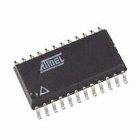
SOIC24 4126F–CAN–12/03 T89C51CC02 141 ...
Page 142
SOIC28 T89C51CC02 142 4126F–CAN–12/03 ...
Page 143
Datasheet Change Log for T89C51CC02 Changes from 4126C- 10/02 to 4126D-04/03 Changes from 4126D- 05/03 to 4126E - 10/03 Changes from 4126E - 10/03 to 4126F - 12/03 4126F–CAN–12/03 1. Changed the endurance of Flash to 100, 000 Write/Erase cycles. ...
Page 144
Table of Features ................................................................................................. 1 Contents Description ............................................................................................ 2 Block Diagram ....................................................................................... 2 Pin Configurations ................................................................................ 3 Pin Description...................................................................................... 5 SFR Mapping ....................................................................................... 10 Clock .................................................................................................... 16 Power Management ............................................................................ 20 Reset Pin .............................................................................................. 20 Data Memory ....................................................................................... 25 EEPROM ...
Page 145
Program/Code Memory ...................................................................... 33 Operation Cross Memory Access ..................................................... 42 Sharing Instructions ........................................................................... 43 In-System Programming (ISP) ........................................................... 45 Serial I/O Port ...................................................................................... 49 Timers/Counters ................................................................................. 55 Timer 2 ................................................................................................. 62 Watchdog Timer .................................................................................. 67 Watchdog Timer During Power-down Mode ...
Page 146
CAN Controller Description ................................................................................ 71 CAN Controller Mailbox and Registers Organization ......................................... 72 CAN Controller Management ............................................................. 73 IT CAN Management.......................................................................................... 74 bit Timing and Baud Rate ................................................................................... 76 Fault Confinement .............................................................................................. 78 Acceptance Filter................................................................................................ 79 Data and Remote Frame ...
Page 147
Ordering Information ........................................................................ 138 Package Drawings ............................................................................ 139 Datasheet Change Log for T89C51CC02 ........................................ 143 Table of Contents ................................................................................... Parameters for Standard Voltage............................................................... 132 DC Parameters for A/D Converter.................................................................... 134 AC Parameters ................................................................................................. 135 VQFP32............................................................................................................ 139 PLCC28 ...
Page 148
... No licenses to patents or other intellectual property of Atmel are granted by the Company in connection with the sale of Atmel products, expressly or by implication. Atmel’s products are not authorized for use as critical components in life support devices or systems. ...