AT89C51CC02UA-RATUM Atmel, AT89C51CC02UA-RATUM Datasheet - Page 140
AT89C51CC02UA-RATUM
Manufacturer Part Number
AT89C51CC02UA-RATUM
Description
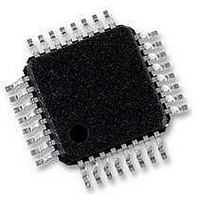
IC 8051 MCU 16K FLASH 32-VQFP
Manufacturer
Atmel
Series
AT89C CANr
Datasheet
1.T89C51CC02CA-TDSIM.pdf
(159 pages)
Specifications of AT89C51CC02UA-RATUM
Core Processor
8051
Core Size
8-Bit
Speed
40MHz
Connectivity
CAN, UART/USART
Peripherals
POR, PWM, WDT
Number Of I /o
20
Program Memory Size
16KB (16K x 8)
Program Memory Type
FLASH
Eeprom Size
2K x 8
Ram Size
512 x 8
Voltage - Supply (vcc/vdd)
3 V ~ 5.5 V
Data Converters
A/D 8x10b
Oscillator Type
External
Operating Temperature
-40°C ~ 85°C
Package / Case
32-TQFP, 32-VQFP
Processor Series
AT89x
Core
8051
Data Bus Width
8 bit
Data Ram Size
512 B
Interface Type
UART
Maximum Clock Frequency
40 MHz
Number Of Programmable I/os
20
Number Of Timers
1
Operating Supply Voltage
3 V to 5.5 V
Maximum Operating Temperature
+ 85 C
Mounting Style
SMD/SMT
3rd Party Development Tools
PK51, CA51, A51, ULINK2
Development Tools By Supplier
CANADAPT28
Minimum Operating Temperature
- 40 C
On-chip Adc
10 bit, 8 Channel
For Use With
AT89OCD-01 - USB EMULATOR FOR AT8XC51 MCU
Lead Free Status / RoHS Status
Lead free / RoHS Compliant
Available stocks
Company
Part Number
Manufacturer
Quantity
Price
Company:

Part Number:
AT89C51CC02UA-RATUM
Manufacturer:
Atmel
Quantity:
1 845


Electrical Characteristics
Absolute Maximum Ratings
DC Parameters for
Standard Voltage
T
Table 114. DC Parameters in Standard Voltage
Notes:
140
A
I = industrial ....................................................... -40°C to 85°C
Storage Temperature ................................... -65°C to + 150°C
Voltage on V
Voltage on Any Pin from V
Power Dissipation ............................................................. 1 W
Symbol
= -40°C to +85°C; V
V
R
V
V
C
V
V
IH1
I
I
I
I
I
CC
RST
PD
TL
OL
OH
IL
LI
IH
IO
IL
(2)
1. Typicals are based on a limited number of samples and are not guaranteed. The values listed are at room temperature.
2. Flash retention is guaranteed with the same formula for V
3. Under steady state (non-transient) conditions, I
AT/T89C51CC02
Maximum I
Parameter
Input Low Voltage
Input High Voltage except XTAL1, RST
Input High Voltage, XTAL1, RST
Output Low Voltage, ports 1, 2, 3 and 4
Output High Voltage, ports 1, 2, 3, 4 and 5
RST Pulldown Resistor
Logical 0 Input Current ports 1, 2, 3 and 4
Input Leakage Current
Logical 1 to 0 Transition Current, ports 1, 2, 3
and 4
Capacitance of I/O Buffer
Power-down Current
Power Supply Current
I
I
CCOP
CCIDLE
CC
from V
(6)
(5)
= 0.7 Freq (MHz) + 3 mA
= 0.6 Freq (MHz) + 2 mA
OL
SS
SS
per port pin: 10 mA
.....................................-0.5V to + 6V
SS
= 0 V; V
.....................-0.5V to V
CC
= 3 volts to 5.5 volts; F = 0 to 40 MHz
(3)
CC
+ 0.2V
OL
0.2 V
V
V
V
0.7 V
must be externally limited as follows:
CC
CC
CC
Min
-0.5
CC
50
- 0.3
- 0.7
- 1.5
CC
Note:
+ 0.9
CC
min down to 0V.
S
Maximum Ratings” may cause permanent damage to
the device. This is a stress rating only and functional
operation of the device at these or any other condi-
tions above those indicated in the operational
sections of this specification is not implied. Exposure
to absolute maximum rating conditions may affect
device reliability.
Power Dissipation value is based on the maximum
allowable die temperature and the thermal resistance
of the package.
tresses at or above those listed under “Absolute
Typ
160
90
(1)
0.2Vcc - 0.1
V
V
CC
CC
Max
-650
0.45
200
±10
400
-50
0.3
1.0
10
+ 0.5
+ 0.5
Unit
kΩ
μA
μA
μA
μA
pF
V
V
V
V
V
V
V
V
V
I
I
I
I
I
I
V
Vin = 0.45V
0.45V < Vin < V
Vin = 2.0V
Fc = 1 MHz
T
3V < V
OL
OL
OL
OH
OH
OH
A
CC
= 25°C
= 100 μA
= 1.6 mA
= 3.5 mA
= -10 μA
= -30 μA
= -60 μA
= 5V ± 10%
Test Conditions
CC
< 5.5V
4126L–CAN–01/08
CC
(4)
Related parts for AT89C51CC02UA-RATUM
Image
Part Number
Description
Manufacturer
Datasheet
Request
R

Part Number:
Description:
Manufacturer:
Atmel Corporation
Datasheet:
Part Number:
Description:
At89c51cc02, T89c51cc02 Enhanced 8-bit Microcontroller With Can Controller And Flash
Manufacturer:
ATMEL Corporation
Datasheet:

Part Number:
Description:
DEV KIT FOR AVR/AVR32
Manufacturer:
Atmel
Datasheet:
Part Number:
Description:
INTERVAL AND WIPE/WASH WIPER CONTROL IC WITH DELAY
Manufacturer:
ATMEL Corporation
Datasheet:
Part Number:
Description:
Low-Voltage Voice-Switched IC for Hands-Free Operation
Manufacturer:
ATMEL Corporation
Datasheet:
Part Number:
Description:
MONOLITHIC INTEGRATED FEATUREPHONE CIRCUIT
Manufacturer:
ATMEL Corporation
Datasheet:
Part Number:
Description:
AM-FM Receiver IC U4255BM-M
Manufacturer:
ATMEL Corporation
Datasheet:
Part Number:
Description:
Monolithic Integrated Feature Phone Circuit
Manufacturer:
ATMEL Corporation
Datasheet:
Part Number:
Description:
Multistandard Video-IF and Quasi Parallel Sound Processing
Manufacturer:
ATMEL Corporation
Datasheet:
Part Number:
Description:
High-performance EE PLD
Manufacturer:
ATMEL Corporation
Datasheet:
Part Number:
Description:
8-bit Flash Microcontroller
Manufacturer:
ATMEL Corporation
Datasheet:
Part Number:
Description:
2-Wire Serial EEPROM
Manufacturer:
ATMEL Corporation
Datasheet: