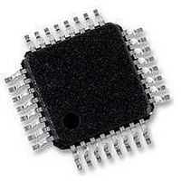
AT89C51CC02UA-RATUM Atmel, AT89C51CC02UA-RATUM Datasheet - Page 26

AT89C51CC02UA-RATUM
Manufacturer Part Number
AT89C51CC02UA-RATUM
Description
IC 8051 MCU 16K FLASH 32-VQFP
Manufacturer
Atmel
Series
AT89C CANr
Datasheet
1.T89C51CC02CA-TDSIM.pdf
(159 pages)
Specifications of AT89C51CC02UA-RATUM
Core Processor
8051
Core Size
8-Bit
Speed
40MHz
Connectivity
CAN, UART/USART
Peripherals
POR, PWM, WDT
Number Of I /o
20
Program Memory Size
16KB (16K x 8)
Program Memory Type
FLASH
Eeprom Size
2K x 8
Ram Size
512 x 8
Voltage - Supply (vcc/vdd)
3 V ~ 5.5 V
Data Converters
A/D 8x10b
Oscillator Type
External
Operating Temperature
-40°C ~ 85°C
Package / Case
32-TQFP, 32-VQFP
Processor Series
AT89x
Core
8051
Data Bus Width
8 bit
Data Ram Size
512 B
Interface Type
UART
Maximum Clock Frequency
40 MHz
Number Of Programmable I/os
20
Number Of Timers
1
Operating Supply Voltage
3 V to 5.5 V
Maximum Operating Temperature
+ 85 C
Mounting Style
SMD/SMT
3rd Party Development Tools
PK51, CA51, A51, ULINK2
Development Tools By Supplier
CANADAPT28
Minimum Operating Temperature
- 40 C
On-chip Adc
10 bit, 8 Channel
For Use With
AT89OCD-01 - USB EMULATOR FOR AT8XC51 MCU
Lead Free Status / RoHS Status
Lead free / RoHS Compliant
Available stocks
Company
Part Number
Manufacturer
Quantity
Price
Company:
Part Number:
AT89C51CC02UA-RATUM
Manufacturer:
Atmel
Quantity:
1 845
Data Memory
Internal Space
Lower 128 Bytes RAM
26
AT/T89C51CC02
The T89C51CC02 provides data memory access in two different spaces:
The internal space mapped in three separate segments:
•
•
•
A fourth internal segment is available but dedicated to Special Function Registers,
SFRs, (addresses 80h to FFh) accessible by direct addressing mode.
Figure 9 shows the internal data memory spaces organization.
Figure 9. Internal memory - RAM
The lower 128 Bytes of RAM (See Figure 10) are accessible from address 00h to 7Fh
using direct or indirect addressing modes. The lowest 32 Bytes are grouped into 4
banks of 8 registers (R0 to R7). Two bits RS0 and RS1 in PSW register (See Table 18)
select which bank is in use according to Table 17. This allows more efficient use of code
space, since register instructions are shorter than instructions that use direct address-
ing, and can be used for context switching in interrupt service routines.
Table 17. Register Bank Selection
The next 16 Bytes above the register banks form a block of bit-addressable memory
space. The C51 instruction set includes a wide selection of singlebit instructions, and
the 128 bits in this area can be directly addressed by these instructions. The bit
addresses in this area are 00h to 7Fh.
The lower 128 Bytes RAM segment.
The upper 128 Bytes RAM segment.
The expanded 256 Bytes RAM segment (XRAM).
RS1
0
0
1
1
FFh
00h
Internal XRAM
256 Bytes
RS0
0
1
0
1
FFh
7Fh
80h
00h
Description
Register bank 0 from 00h to 07h
Register bank 0 from 08h to 0Fh
Register bank 0 from 10h to 17h
Register bank 0 from 18h to 1Fh
Indirect Addressing
Direct or Indirect
Internal RAM
Internal RAM
Addressing
128 Bytes
128 Bytes
Upper
Lower
FFh
80h
Direct Addressing
Registers
Function
Special
4126L–CAN–01/08


