MC908JB16DWE Freescale Semiconductor, MC908JB16DWE Datasheet - Page 249
MC908JB16DWE
Manufacturer Part Number
MC908JB16DWE
Description
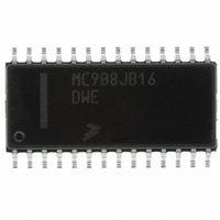
IC MCU 16K FLASH 6MHZ USB 28SOIC
Manufacturer
Freescale Semiconductor
Series
HC08r
Specifications of MC908JB16DWE
Core Processor
HC08
Core Size
8-Bit
Speed
6MHz
Connectivity
SCI, USB
Peripherals
LED, LVD, POR, PWM
Number Of I /o
21
Program Memory Size
16KB (16K x 8)
Program Memory Type
FLASH
Ram Size
384 x 8
Voltage - Supply (vcc/vdd)
4 V ~ 5.5 V
Oscillator Type
Internal
Operating Temperature
0°C ~ 70°C
Package / Case
28-SOIC (7.5mm Width)
Processor Series
HC08JB
Core
HC08
Data Bus Width
8 bit
Data Ram Size
384 B
Interface Type
I2C/SCI/SPI/USB
Maximum Clock Frequency
12 MHz
Number Of Programmable I/os
21
Number Of Timers
4
Operating Supply Voltage
5.5 V
Maximum Operating Temperature
+ 70 C
Mounting Style
SMD/SMT
Development Tools By Supplier
FSICEBASE, DEMO908GZ60E, M68EML08GZE, KITUSBSPIDGLEVME, KITUSBSPIEVME, KIT33810EKEVME
Minimum Operating Temperature
0 C
Controller Family/series
HC08
No. Of I/o's
21
Ram Memory Size
384Byte
Cpu Speed
8MHz
No. Of Timers
2
Embedded Interface Type
I2C, SCI, SPI
Rohs Compliant
Yes
Lead Free Status / RoHS Status
Lead free / RoHS Compliant
Eeprom Size
-
Data Converters
-
Lead Free Status / Rohs Status
Lead free / RoHS Compliant
Available stocks
Company
Part Number
Manufacturer
Quantity
Price
Company:

Part Number:
MC908JB16DWE
Manufacturer:
FREESCALE
Quantity:
1 831
Part Number:
MC908JB16DWE
Manufacturer:
FRE/MOT
Quantity:
20 000


13.3 Functional Description
MC68HC908JB16
Freescale Semiconductor
$0054
$0055
$0056
$0057
$0058
$0059
PLL2 N & R Divider Select
Phase Detector Control
PLL1 N Divider Select
PLL1 R Divider Select
PLL2 N Divider Select
PLL2 R Divider Select
Register High
Register Low
Register Low
Register Low
Register Low
—
Rev. 1.1
(PNRH2)
(PNSL1)
(PRSL1)
(PNSL1)
(PRSL2)
Register
(PDCR)
Figure 13-2
this MCU.
The two CGMs are independently programmable, with their respective
outputs at the CGMOUT1 and CGMOUT2 pins.
The following paragraphs describes the CGM circuit blocks and internal
signals.
Reset:
Reset:
Reset:
Reset:
Reset:
Reset:
Read:
Read:
Read:
Read:
Read:
Read:
Write:
Write:
Write:
Write:
Write:
Write:
Figure 13-1. CGM I/O Register Summary
VDS2_11 VDS2_10
VDS1_7
RDS1_7
VDS2_7
RDS2_7
PHD_7
0
1
0
0
1
1
Clock Generator Module (CGM)
shows the structure of one CGM. There are two CGMs in
RDS1_6
RDS2_6
VDS1_6
VDS2_6
PHD_6
1
0
0
1
0
0
RDS1_5
RDS2_5
VDS1_5
VDS2_9
VDS2_5
PHD_5
1
0
1
1
0
0
VDS1_4
RDS1_4
VDS2_8
VDS2_4
RDS2_4
PHD_4
1
1
0
1
1
1
VDS1_3
RDS1_3
VDS2_3
RDS2_3
PHD_3
1
0
0
0
1
0
0
Clock Generator Module (CGM)
VDS1_2
RDS1_2
VDS2_2
RDS2_2
PHD_2
1
0
0
0
1
0
0
RDS1_1
RDS2_9
RDS2_1
VDS1_1
VDS2_1
PHD_1
0
0
0
0
0
0
Technical Data
RDS1_0
RDS2_8
RDS2_0
VDS1_0
VDS2_0
PHD_0
1
0
0
1
0
0
249
Related parts for MC908JB16DWE
Image
Part Number
Description
Manufacturer
Datasheet
Request
R

Part Number:
Description:
Manufacturer:
Freescale Semiconductor, Inc
Datasheet:
Part Number:
Description:
Manufacturer:
Freescale Semiconductor, Inc
Datasheet:
Part Number:
Description:
Manufacturer:
Freescale Semiconductor, Inc
Datasheet:
Part Number:
Description:
Manufacturer:
Freescale Semiconductor, Inc
Datasheet:
Part Number:
Description:
Manufacturer:
Freescale Semiconductor, Inc
Datasheet:
Part Number:
Description:
Manufacturer:
Freescale Semiconductor, Inc
Datasheet:
Part Number:
Description:
Manufacturer:
Freescale Semiconductor, Inc
Datasheet:
Part Number:
Description:
Manufacturer:
Freescale Semiconductor, Inc
Datasheet:
Part Number:
Description:
Manufacturer:
Freescale Semiconductor, Inc
Datasheet:
Part Number:
Description:
Manufacturer:
Freescale Semiconductor, Inc
Datasheet:
Part Number:
Description:
Manufacturer:
Freescale Semiconductor, Inc
Datasheet:
Part Number:
Description:
Manufacturer:
Freescale Semiconductor, Inc
Datasheet:
Part Number:
Description:
Manufacturer:
Freescale Semiconductor, Inc
Datasheet:
Part Number:
Description:
Manufacturer:
Freescale Semiconductor, Inc
Datasheet:
Part Number:
Description:
Manufacturer:
Freescale Semiconductor, Inc
Datasheet: