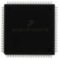
MC9S12E128CPVE Freescale Semiconductor, MC9S12E128CPVE Datasheet - Page 218

MC9S12E128CPVE
Manufacturer Part Number
MC9S12E128CPVE
Description
IC MCU 128K FLASH 25MHZ 112-LQFP
Manufacturer
Freescale Semiconductor
Series
HCS12r
Specifications of MC9S12E128CPVE
Core Processor
HCS12
Core Size
16-Bit
Speed
25MHz
Connectivity
EBI/EMI, I²C, SCI, SPI
Peripherals
POR, PWM, WDT
Number Of I /o
91
Program Memory Size
128KB (128K x 8)
Program Memory Type
FLASH
Ram Size
8K x 8
Voltage - Supply (vcc/vdd)
2.35 V ~ 2.75 V
Data Converters
A/D 16x10b; D/A 2x8b
Oscillator Type
Internal
Operating Temperature
-40°C ~ 85°C
Package / Case
112-LQFP
Processor Series
S12E
Core
HCS12
Data Bus Width
16 bit
Data Ram Size
8 KB
Interface Type
SCI/SPI
Maximum Clock Frequency
25 MHz
Number Of Programmable I/os
92
Number Of Timers
12
Operating Supply Voltage
3.135 V to 5.5 V
Maximum Operating Temperature
+ 85 C
Mounting Style
SMD/SMT
3rd Party Development Tools
EWHCS12
Minimum Operating Temperature
- 40 C
On-chip Adc
16-ch x 10-bit
On-chip Dac
2-ch x 8-bit
Controller Family/series
HCS12/S12X
No. Of I/o's
90
Ram Memory Size
8KB
Cpu Speed
25MHz
No. Of Timers
4
Embedded Interface Type
I2C, SCI, SPI
Rohs Compliant
Yes
For Use With
M68EVB912E128 - BOARD EVAL FOR MC9S12E128/64
Lead Free Status / RoHS Status
Lead free / RoHS Compliant
Eeprom Size
-
Lead Free Status / Rohs Status
Lead free / RoHS Compliant
Available stocks
Company
Part Number
Manufacturer
Quantity
Price
Company:
Part Number:
MC9S12E128CPVE
Manufacturer:
Freescale Semiconductor
Quantity:
10 000
- Current page: 218 of 606
- Download datasheet (4Mb)
Chapter 6 Analog-to-Digital Converter (ATD10B16CV2)
6.3.2.6
This register selects the type of conversion sequence and the analog input channels sampled. Writes to this
register will abort current conversion sequence and start a new conversion sequence. If external trigger is
enabled (ETRIGE = 1) an initial write to ATDCTL5 is required to allow starting of a conversion sequence
which will then occur on each trigger event. Start of conversion means the beginning of the sampling
phase.
Read: Anytime
Write: Anytime
218
Reset
DSGN
SCAN
MULT
Field
DJM
W
7
6
5
4
R
DJM
ATD Control Register 5 (ATDCTL5)
0
7
Result Register Data Justification — This bit controls justification of conversion data in the result registers.
See
0 Left justified data in the result registers.
1 Right justified data in the result registers.
Result Register Data Signed or Unsigned Representation — This bit selects between signed and unsigned
conversion data representation in the result registers. Signed data is represented as 2’s complement. Signed
data is not available in right justification. See <st-bold>6.3.2.16 ATD Conversion Result Registers (ATDDRx)
for details.
0 Unsigned data representation in the result registers.
1 Signed data representation in the result registers.
Table 6-11
Table 6-12
signal range between 0 and 5.12 Volts.
Continuous Conversion Sequence Mode — This bit selects whether conversion sequences are performed
continuously or only once. If external trigger is enabled (ETRIGE=1) setting this bit has no effect, that means
each trigger event starts a single conversion sequence.
0 Single conversion sequence
1 Continuous conversion sequences (scan mode)
Multi-Channel Sample Mode — When MULT is 0, the ATD sequence controller samples only from the
specified analog input channel for an entire conversion sequence. The analog channel is selected by channel
selection code (control bits CD/CC/CB/CA located in ATDCTL5). When MULT is 1, the ATD sequence controller
samples across channels. The number of channels sampled is determined by the sequence length value (S8C,
S4C, S2C, S1C). The first analog channel examined is determined by channel selection code (CC, CB, CA
control bits); subsequent channels sampled in the sequence are determined by incrementing the channel
selection code or wrapping around to AN0 (channel 0.
0 Sample only one channel
1 Sample across several channels
Section 6.3.2.16, “ATD Conversion Result Registers (ATDDRx)”
summarizes the result data formats available and how they are set up using the control bits.
illustrates the difference between the signed and unsigned, left justified output codes for an input
DSGN
0
6
Figure 6-8. ATD Control Register 5 (ATDCTL5)
Table 6-10. ATDCTL5 Field Descriptions
SCAN
MC9S12E128 Data Sheet, Rev. 1.07
0
5
MULT
0
4
Description
CD
0
3
for details.
CC
0
2
Freescale Semiconductor
CB
0
1
CA
0
0
Related parts for MC9S12E128CPVE
Image
Part Number
Description
Manufacturer
Datasheet
Request
R
Part Number:
Description:
Manufacturer:
Freescale Semiconductor, Inc
Datasheet:
Part Number:
Description:
Manufacturer:
Freescale Semiconductor, Inc
Datasheet:
Part Number:
Description:
Manufacturer:
Freescale Semiconductor, Inc
Datasheet:
Part Number:
Description:
Manufacturer:
Freescale Semiconductor, Inc
Datasheet:
Part Number:
Description:
Manufacturer:
Freescale Semiconductor, Inc
Datasheet:
Part Number:
Description:
Manufacturer:
Freescale Semiconductor, Inc
Datasheet:
Part Number:
Description:
Manufacturer:
Freescale Semiconductor, Inc
Datasheet:
Part Number:
Description:
Manufacturer:
Freescale Semiconductor, Inc
Datasheet:
Part Number:
Description:
Manufacturer:
Freescale Semiconductor, Inc
Datasheet:
Part Number:
Description:
Manufacturer:
Freescale Semiconductor, Inc
Datasheet:
Part Number:
Description:
Manufacturer:
Freescale Semiconductor, Inc
Datasheet:
Part Number:
Description:
Manufacturer:
Freescale Semiconductor, Inc
Datasheet:
Part Number:
Description:
Manufacturer:
Freescale Semiconductor, Inc
Datasheet:
Part Number:
Description:
Manufacturer:
Freescale Semiconductor, Inc
Datasheet:
Part Number:
Description:
Manufacturer:
Freescale Semiconductor, Inc
Datasheet:


