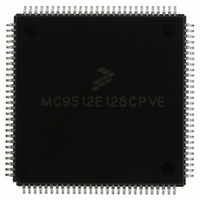
MC9S12E128CPVE Freescale Semiconductor, MC9S12E128CPVE Datasheet - Page 254

MC9S12E128CPVE
Manufacturer Part Number
MC9S12E128CPVE
Description
IC MCU 128K FLASH 25MHZ 112-LQFP
Manufacturer
Freescale Semiconductor
Series
HCS12r
Specifications of MC9S12E128CPVE
Core Processor
HCS12
Core Size
16-Bit
Speed
25MHz
Connectivity
EBI/EMI, I²C, SCI, SPI
Peripherals
POR, PWM, WDT
Number Of I /o
91
Program Memory Size
128KB (128K x 8)
Program Memory Type
FLASH
Ram Size
8K x 8
Voltage - Supply (vcc/vdd)
2.35 V ~ 2.75 V
Data Converters
A/D 16x10b; D/A 2x8b
Oscillator Type
Internal
Operating Temperature
-40°C ~ 85°C
Package / Case
112-LQFP
Processor Series
S12E
Core
HCS12
Data Bus Width
16 bit
Data Ram Size
8 KB
Interface Type
SCI/SPI
Maximum Clock Frequency
25 MHz
Number Of Programmable I/os
92
Number Of Timers
12
Operating Supply Voltage
3.135 V to 5.5 V
Maximum Operating Temperature
+ 85 C
Mounting Style
SMD/SMT
3rd Party Development Tools
EWHCS12
Minimum Operating Temperature
- 40 C
On-chip Adc
16-ch x 10-bit
On-chip Dac
2-ch x 8-bit
Controller Family/series
HCS12/S12X
No. Of I/o's
90
Ram Memory Size
8KB
Cpu Speed
25MHz
No. Of Timers
4
Embedded Interface Type
I2C, SCI, SPI
Rohs Compliant
Yes
For Use With
M68EVB912E128 - BOARD EVAL FOR MC9S12E128/64
Lead Free Status / RoHS Status
Lead free / RoHS Compliant
Eeprom Size
-
Lead Free Status / Rohs Status
Lead free / RoHS Compliant
Available stocks
Company
Part Number
Manufacturer
Quantity
Price
Company:
Part Number:
MC9S12E128CPVE
Manufacturer:
Freescale Semiconductor
Quantity:
10 000
- Current page: 254 of 606
- Download datasheet (4Mb)
Chapter 8 Serial Communication Interface (SCIV3)
8.3.2.4
The SCISR1 and SCISR2 registers provide inputs to the MCU for generation of SCI interrupts. Also, these
registers can be polled by the MCU to check the status of these bits. The flag-clearing procedures require
that the status register be read followed by a read or write to the SCI data register. It is permissible to
execute other instructions between the two steps as long as it does not compromise the handling of I/O.
Note that the order of operations is important for flag clearing.
Read: anytime
Write: has no meaning or effect
254
Reset
RDRF
TDRE
Field
IDLE
TC
7
6
5
4
W
R
TDRE
Transmit Data Register Empty Flag — TDRE is set when the transmit shift register receives a byte from the
SCI data register. When TDRE is 1, the transmit data register (SCIDRH/L) is empty and can receive a new value
to transmit.Clear TDRE by reading SCI status register 1 (SCISR1), with TDRE set and then writing to SCI data
register low (SCIDRL).
0 No byte transferred to transmit shift register
1 Byte transferred to transmit shift register; transmit data register empty
Transmit Complete Flag — TC is set low when there is a transmission in progress or when a preamble or break
character is loaded. TC is set high when the TDRE flag is set and no data, preamble, or break character is being
transmitted.When TC is set, the TXD pin becomes idle (logic 1). Clear TC by reading SCI status register 1
(SCISR1) with TC set and then writing to SCI data register low (SCIDRL). TC is cleared automatically when data,
preamble, or break is queued and ready to be sent. TC is cleared in the event of a simultaneous set and clear of
the TC flag (transmission not complete).
0 Transmission in progress
1 No transmission in progress
Receive Data Register Full Flag — RDRF is set when the data in the receive shift register transfers to the SCI
data register. Clear RDRF by reading SCI status register 1 (SCISR1) with RDRF set and then reading SCI data
register low (SCIDRL).
0 Data not available in SCI data register
1 Received data available in SCI data register
Idle Line Flag
on the receiver input. After the IDLE flag is cleared, a valid frame must again set the RDRF flag before an idle
condition can set the IDLE flag.Clear IDLE by reading SCI status register 1 (SCISR1) with IDLE set and then
reading SCI data register low (SCIDRL).
0 Receiver input is either active now or has never become active since the IDLE flag was last cleared
1 Receiver input has become idle
SCI Status Register 1 (SCISR1)
1
7
= Unimplemented or Reserved
1
TC
— IDLE is set when 10 consecutive logic 1s (if M = 0) or 11 consecutive logic 1s (if M = 1) appear
1
6
Figure 8-7. SCI Status Register 1 (SCISR1)
Table 8-7. SCISR1 Field Descriptions
RDRF
MC9S12E128 Data Sheet, Rev. 1.07
0
5
IDLE
0
4
Description
OR
0
3
NF
0
2
Freescale Semiconductor
FE
0
1
PF
0
0
Related parts for MC9S12E128CPVE
Image
Part Number
Description
Manufacturer
Datasheet
Request
R
Part Number:
Description:
Manufacturer:
Freescale Semiconductor, Inc
Datasheet:
Part Number:
Description:
Manufacturer:
Freescale Semiconductor, Inc
Datasheet:
Part Number:
Description:
Manufacturer:
Freescale Semiconductor, Inc
Datasheet:
Part Number:
Description:
Manufacturer:
Freescale Semiconductor, Inc
Datasheet:
Part Number:
Description:
Manufacturer:
Freescale Semiconductor, Inc
Datasheet:
Part Number:
Description:
Manufacturer:
Freescale Semiconductor, Inc
Datasheet:
Part Number:
Description:
Manufacturer:
Freescale Semiconductor, Inc
Datasheet:
Part Number:
Description:
Manufacturer:
Freescale Semiconductor, Inc
Datasheet:
Part Number:
Description:
Manufacturer:
Freescale Semiconductor, Inc
Datasheet:
Part Number:
Description:
Manufacturer:
Freescale Semiconductor, Inc
Datasheet:
Part Number:
Description:
Manufacturer:
Freescale Semiconductor, Inc
Datasheet:
Part Number:
Description:
Manufacturer:
Freescale Semiconductor, Inc
Datasheet:
Part Number:
Description:
Manufacturer:
Freescale Semiconductor, Inc
Datasheet:
Part Number:
Description:
Manufacturer:
Freescale Semiconductor, Inc
Datasheet:
Part Number:
Description:
Manufacturer:
Freescale Semiconductor, Inc
Datasheet:


