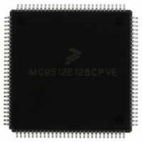
MC9S12E128CPVE Freescale Semiconductor, MC9S12E128CPVE Datasheet - Page 443

MC9S12E128CPVE
Manufacturer Part Number
MC9S12E128CPVE
Description
IC MCU 128K FLASH 25MHZ 112-LQFP
Manufacturer
Freescale Semiconductor
Series
HCS12r
Specifications of MC9S12E128CPVE
Core Processor
HCS12
Core Size
16-Bit
Speed
25MHz
Connectivity
EBI/EMI, I²C, SCI, SPI
Peripherals
POR, PWM, WDT
Number Of I /o
91
Program Memory Size
128KB (128K x 8)
Program Memory Type
FLASH
Ram Size
8K x 8
Voltage - Supply (vcc/vdd)
2.35 V ~ 2.75 V
Data Converters
A/D 16x10b; D/A 2x8b
Oscillator Type
Internal
Operating Temperature
-40°C ~ 85°C
Package / Case
112-LQFP
Processor Series
S12E
Core
HCS12
Data Bus Width
16 bit
Data Ram Size
8 KB
Interface Type
SCI/SPI
Maximum Clock Frequency
25 MHz
Number Of Programmable I/os
92
Number Of Timers
12
Operating Supply Voltage
3.135 V to 5.5 V
Maximum Operating Temperature
+ 85 C
Mounting Style
SMD/SMT
3rd Party Development Tools
EWHCS12
Minimum Operating Temperature
- 40 C
On-chip Adc
16-ch x 10-bit
On-chip Dac
2-ch x 8-bit
Controller Family/series
HCS12/S12X
No. Of I/o's
90
Ram Memory Size
8KB
Cpu Speed
25MHz
No. Of Timers
4
Embedded Interface Type
I2C, SCI, SPI
Rohs Compliant
Yes
For Use With
M68EVB912E128 - BOARD EVAL FOR MC9S12E128/64
Lead Free Status / RoHS Status
Lead free / RoHS Compliant
Eeprom Size
-
Lead Free Status / Rohs Status
Lead free / RoHS Compliant
Available stocks
Company
Part Number
Manufacturer
Quantity
Price
Company:
Part Number:
MC9S12E128CPVE
Manufacturer:
Freescale Semiconductor
Quantity:
10 000
- Current page: 443 of 606
- Download datasheet (4Mb)
14.3.2
The following paragraphs describe, in address order, all the VREG3V3V2 registers and their individual
bits.
14.3.2.1
The VREGCTRL register allows to separately enable features of VREG3V3V2.
14.4
Block VREG3V3V2 is a voltage regulator as depicted in
are the regulator core (REG), a low-voltage detect module (LVD), a power-on reset module (POR) and a
low-voltage reset module (LVR). There is also the regulator control block (CTRL) which represents the
interface to the digital core logic but also manages the operating modes of VREG3V3V2.
14.4.1
VREG3V3V2, respectively its regulator core has two parallel, independent regulation loops (REG1 and
REG2) that differ only in the amount of current that can be sourced to the connected loads. Therefore, only
REG1 providing the supply at V
Freescale Semiconductor
Reset
LVDS
Field
LVIE
LVIF
2
1
0
W
R
Functional Description
Register Descriptions
REG — Regulator Core
Low-Voltage Detect Status Bit — This read-only status bit reflects the input voltage. Writes have no effect.
0 Input voltage V
1 Input voltage V
Low-Voltage Interrupt Enable Bit
0 Interrupt request is disabled.
1 Interrupt will be requested whenever LVIF is set.
Low-Voltage Interrupt Flag — LVIF is set to 1 when LVDS status bit changes. This flag can only be cleared by
writing a 1. Writing a 0 has no effect. If enabled (LVIE = 1), LVIF causes an interrupt request.
0 No change in LVDS bit.
1 LVDS bit has changed.
VREG3V3V2 — Control Register (VREGCTRL)
0
0
7
On entering the reduced-power mode the LVIF is not cleared by the
VREG3V3V2.
= Unimplemented or Reserved
Figure 14-2. VREG3V3 — Control Register (VREGCTRL)
0
0
6
DDA
DDA
is above level V
is below level V
DD
Table 14-3. MCCTL1 Field Descriptions
/V
MC9S12E128 Data Sheet, Rev. 1.07
SS
0
0
5
is explained. The principle is also valid for REG2.
LVIA
LVID
and FPM.
or RPM or shutdown mode.
NOTE
0
0
4
Description
Figure
Chapter 14 Dual Output Voltage Regulator (VREG3V3V2)
0
0
3
14-1. The regulator functional elements
LVDS
0
2
LVIE
0
1
LVIF
0
0
443
Related parts for MC9S12E128CPVE
Image
Part Number
Description
Manufacturer
Datasheet
Request
R
Part Number:
Description:
Manufacturer:
Freescale Semiconductor, Inc
Datasheet:
Part Number:
Description:
Manufacturer:
Freescale Semiconductor, Inc
Datasheet:
Part Number:
Description:
Manufacturer:
Freescale Semiconductor, Inc
Datasheet:
Part Number:
Description:
Manufacturer:
Freescale Semiconductor, Inc
Datasheet:
Part Number:
Description:
Manufacturer:
Freescale Semiconductor, Inc
Datasheet:
Part Number:
Description:
Manufacturer:
Freescale Semiconductor, Inc
Datasheet:
Part Number:
Description:
Manufacturer:
Freescale Semiconductor, Inc
Datasheet:
Part Number:
Description:
Manufacturer:
Freescale Semiconductor, Inc
Datasheet:
Part Number:
Description:
Manufacturer:
Freescale Semiconductor, Inc
Datasheet:
Part Number:
Description:
Manufacturer:
Freescale Semiconductor, Inc
Datasheet:
Part Number:
Description:
Manufacturer:
Freescale Semiconductor, Inc
Datasheet:
Part Number:
Description:
Manufacturer:
Freescale Semiconductor, Inc
Datasheet:
Part Number:
Description:
Manufacturer:
Freescale Semiconductor, Inc
Datasheet:
Part Number:
Description:
Manufacturer:
Freescale Semiconductor, Inc
Datasheet:
Part Number:
Description:
Manufacturer:
Freescale Semiconductor, Inc
Datasheet:


