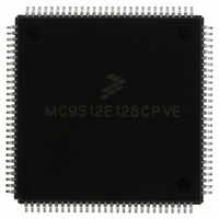
MC9S12E128CPVE Freescale Semiconductor, MC9S12E128CPVE Datasheet - Page 71

MC9S12E128CPVE
Manufacturer Part Number
MC9S12E128CPVE
Description
IC MCU 128K FLASH 25MHZ 112-LQFP
Manufacturer
Freescale Semiconductor
Series
HCS12r
Specifications of MC9S12E128CPVE
Core Processor
HCS12
Core Size
16-Bit
Speed
25MHz
Connectivity
EBI/EMI, I²C, SCI, SPI
Peripherals
POR, PWM, WDT
Number Of I /o
91
Program Memory Size
128KB (128K x 8)
Program Memory Type
FLASH
Ram Size
8K x 8
Voltage - Supply (vcc/vdd)
2.35 V ~ 2.75 V
Data Converters
A/D 16x10b; D/A 2x8b
Oscillator Type
Internal
Operating Temperature
-40°C ~ 85°C
Package / Case
112-LQFP
Processor Series
S12E
Core
HCS12
Data Bus Width
16 bit
Data Ram Size
8 KB
Interface Type
SCI/SPI
Maximum Clock Frequency
25 MHz
Number Of Programmable I/os
92
Number Of Timers
12
Operating Supply Voltage
3.135 V to 5.5 V
Maximum Operating Temperature
+ 85 C
Mounting Style
SMD/SMT
3rd Party Development Tools
EWHCS12
Minimum Operating Temperature
- 40 C
On-chip Adc
16-ch x 10-bit
On-chip Dac
2-ch x 8-bit
Controller Family/series
HCS12/S12X
No. Of I/o's
90
Ram Memory Size
8KB
Cpu Speed
25MHz
No. Of Timers
4
Embedded Interface Type
I2C, SCI, SPI
Rohs Compliant
Yes
For Use With
M68EVB912E128 - BOARD EVAL FOR MC9S12E128/64
Lead Free Status / RoHS Status
Lead free / RoHS Compliant
Eeprom Size
-
Lead Free Status / Rohs Status
Lead free / RoHS Compliant
Available stocks
Company
Part Number
Manufacturer
Quantity
Price
Company:
Part Number:
MC9S12E128CPVE
Manufacturer:
Freescale Semiconductor
Quantity:
10 000
- Current page: 71 of 606
- Download datasheet (4Mb)
1.4.37
PS0 is a general purpose input or output. When the Serial Communications Interface 0 (SCI0) receiver is
enabled the PS0 pin is configured as the receive pin RXD0 of SCI0. While in reset and immediately out of
reset the PS0 pin is configured as a high impedance input pin. Consult the Port Integration Module (PIM)
PIM_9E128 block description chapter and the SCI block description chapter for information about pin
configurations.
1.4.38
PT[7:4] are general purpose input or output pins. When the Timer system 1 (TIM1) is enabled they can
also be configured as the TIM1 input capture or output compare pins IOC1[7-4]. While in reset and
immediately out of reset the PT[7:4] pins are configured as a high impedance input pins. Consult the Port
Integration Module (PIM) PIM_9E128 block description chapter and the TIM_16B4C block description
chapter for information about pin configurations.
1.4.39
PT[3:0] are general purpose input or output pins. When the Timer system 0 (TIM0) is enabled they can
also be configured as the TIM0 input capture or output compare pins IOC0[7-4]. While in reset and
immediately out of reset the PT[3:0] pins are configured as a high impedance input pins. Consult the Port
Integration Module (PIM) PIM_9E128 block description chapter and the TIM_16B4C block description
chapter for information about pin configurations.
1.4.40
PU[7:6] are general purpose input or output pins. While in reset and immediately out of reset the PU[7:6]
pins are configured as a high impedance input pins. Consult the Port Integration Module (PIM)
PIM_9E128 for information about pin configurations. PU[7:6] are not available in the 80 pin package
version.
1.4.41
PU[5:4] are general purpose input or output pins. When the Pulse Width Modulator (PWM) is enabled the
PU[5:4] output pins, individually or as a pair, can be configured as PW1[5:4] outputs. While in reset and
immediately out of reset the PU[5:4] pins are configured as a high impedance input pins. Consult the Port
Integration Module (PIM) PIM_9E128 block description chapter and the PWM_8B6C block description
chapter for information about pin configurations. PU[5:4] are not available in the 80 pin package version.
1.4.42
PU[3:0] are general purpose input or output pins. When the Timer system 2 (TIM2) is enabled they can
also be configured as the TIM2 input capture or output compare pins IOC2[7-4]. When the Pulse Width
Modulator (PWM) is enabled the PU[3:0] output pins, individually or as a pair, can be configured as
PW1[3:0] outputs. The MODRR register in the Port Integration Module determines if the TIM2 or PWM
function is selected. While in reset and immediately out of reset the PU[3:0] pins are configured as a high
Freescale Semiconductor
PS0 / RXD0 — Port S I/O Pin 0
PT[7:4] / IOC1[7:4]— Port T I/O Pins [7:4]
PT[3:0] / IOC0[7:4]— Port T I/O Pins [3:0]
PU[7:6] — Port U I/O Pins [7:6]
PU[5:4] / PW1[5:4] — Port U I/O Pins [5:4]
PU[3:0] / IOC2[7:4]/PW1[3:0] — Port U I/O Pins [3:0]
MC9S12E128 Data Sheet, Rev. 1.07
Chapter 1 MC9S12E128 Device Overview (MC9S12E128DGV1)
71
Related parts for MC9S12E128CPVE
Image
Part Number
Description
Manufacturer
Datasheet
Request
R
Part Number:
Description:
Manufacturer:
Freescale Semiconductor, Inc
Datasheet:
Part Number:
Description:
Manufacturer:
Freescale Semiconductor, Inc
Datasheet:
Part Number:
Description:
Manufacturer:
Freescale Semiconductor, Inc
Datasheet:
Part Number:
Description:
Manufacturer:
Freescale Semiconductor, Inc
Datasheet:
Part Number:
Description:
Manufacturer:
Freescale Semiconductor, Inc
Datasheet:
Part Number:
Description:
Manufacturer:
Freescale Semiconductor, Inc
Datasheet:
Part Number:
Description:
Manufacturer:
Freescale Semiconductor, Inc
Datasheet:
Part Number:
Description:
Manufacturer:
Freescale Semiconductor, Inc
Datasheet:
Part Number:
Description:
Manufacturer:
Freescale Semiconductor, Inc
Datasheet:
Part Number:
Description:
Manufacturer:
Freescale Semiconductor, Inc
Datasheet:
Part Number:
Description:
Manufacturer:
Freescale Semiconductor, Inc
Datasheet:
Part Number:
Description:
Manufacturer:
Freescale Semiconductor, Inc
Datasheet:
Part Number:
Description:
Manufacturer:
Freescale Semiconductor, Inc
Datasheet:
Part Number:
Description:
Manufacturer:
Freescale Semiconductor, Inc
Datasheet:
Part Number:
Description:
Manufacturer:
Freescale Semiconductor, Inc
Datasheet:


