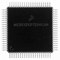
MC9S12XDT256CAA Freescale Semiconductor, MC9S12XDT256CAA Datasheet - Page 1131

MC9S12XDT256CAA
Manufacturer Part Number
MC9S12XDT256CAA
Description
IC MCU 256K FLASH 80-QFP
Manufacturer
Freescale Semiconductor
Series
HCS12r
Datasheet
1.MC9S12XD64CAA.pdf
(1348 pages)
Specifications of MC9S12XDT256CAA
Core Processor
HCS12X
Core Size
16-Bit
Speed
80MHz
Connectivity
CAN, EBI/EMI, I²C, IrDA, LIN, SCI, SPI
Peripherals
LVD, POR, PWM, WDT
Number Of I /o
59
Program Memory Size
256KB (256K x 8)
Program Memory Type
FLASH
Eeprom Size
4K x 8
Ram Size
16K x 8
Voltage - Supply (vcc/vdd)
2.35 V ~ 5.5 V
Data Converters
A/D 8x10b
Oscillator Type
External
Operating Temperature
-40°C ~ 85°C
Package / Case
80-QFP
Processor Series
S12XD
Core
HCS12
Data Bus Width
16 bit
Data Ram Size
16 KB
Interface Type
CAN/I2C/SCI/SPI
Maximum Clock Frequency
40 MHz
Number Of Programmable I/os
59
Number Of Timers
12
Maximum Operating Temperature
+ 85 C
Mounting Style
SMD/SMT
3rd Party Development Tools
EWHCS12
Development Tools By Supplier
EVB9S12XDP512E
Minimum Operating Temperature
- 40 C
On-chip Adc
8-ch x 10-bit
Lead Free Status / RoHS Status
Lead free / RoHS Compliant
Available stocks
Company
Part Number
Manufacturer
Quantity
Price
Company:
Part Number:
MC9S12XDT256CAA
Manufacturer:
Freescale Semiconductor
Quantity:
10 000
Company:
Part Number:
MC9S12XDT256CAAR
Manufacturer:
Freescale Semiconductor
Quantity:
10 000
- Current page: 1131 of 1348
- Download datasheet (8Mb)
27.4.2.2
The data compress operation will check Flash code integrity by compressing data from a selected portion
of the Flash memory into a signature analyzer.
An example flow to execute the data compress operation is shown in
command write sequence is as follows:
After launching the data compress command, the CCIF flag in the FSTAT register will set after the data
compress operation has completed. The number of bus cycles required to execute the data compress
operation is equal to two times the number of consecutive words to compress plus the number of Flash
blocks simultaneously compressed plus 18 bus cycles as measured from the time the CBEIF flag is cleared
until the CCIF flag is set. Once the CCIF flag is set, the signature generated by the data compress operation
is available in the FDATA registers. The signature in the FDATA registers can be compared to the expected
signature to determine the integrity of the selected data stored in the selected Flash memory. If the last
address of a Flash block is reached during the data compress operation, data compression will continue
with the starting address of the same Flash block. The MRDS bits in the FTSTMOD register will determine
the sense-amp margin setting during the data compress operation.
In order to take corrective action, it is recommended that the data compress command be executed on a
Flash sector or subset of a Flash sector. If the data compress operation on a Flash sector returns an invalid
signature, the Flash sector should be erased using the sector erase command and then reprogrammed using
the program command.
The data compress command can be used to verify that a sector or sequential set of sectors are erased.
Freescale Semiconductor
1. Write to a Flash block address to start the command write sequence for the data compress
2. Write the data compress command, 0x06, to the FCMD register.
3. Clear the CBEIF flag in the FSTAT register by writing a 1 to CBEIF to launch the data compress
command. The address written determines the starting address for the data compress operation and
the data written determines the number of consecutive words to compress. If the data value written
is 0x0000, 64K addresses or 128 Kbytes will be compressed. Multiple Flash blocks can be
simultaneously compressed by writing to the same relative address in each Flash block. If more
than one Flash block is written to in this step, the first data written will determine the number of
consecutive words to compress in each selected Flash block.
command.
Data Compress Command
Since the FDATA registers (or data buffer) are written to as part of the data
compress operation, a command write sequence is not allowed to be
buffered behind a data compress command write sequence. The CBEIF flag
will not set after launching the data compress command to indicate that a
command should not be buffered behind it. If an attempt is made to start a
new command write sequence with a data compress operation active, the
ACCERR flag in the FSTAT register will be set. A new command write
sequence should only be started after reading the signature stored in the
FDATA registers.
MC9S12XDP512 Data Sheet, Rev. 2.21
NOTE
Chapter 27 512 Kbyte Flash Module (S12XFTX512K4V2)
Figure
27-26. The data compress
1133
Related parts for MC9S12XDT256CAA
Image
Part Number
Description
Manufacturer
Datasheet
Request
R

Part Number:
Description:
16-BIT MICROPROCESSOR FAMILY
Manufacturer:
FREESCALE [Freescale Semiconductor, Inc]
Datasheet:
Part Number:
Description:
Manufacturer:
Freescale Semiconductor, Inc
Datasheet:
Part Number:
Description:
Manufacturer:
Freescale Semiconductor, Inc
Datasheet:
Part Number:
Description:
Manufacturer:
Freescale Semiconductor, Inc
Datasheet:
Part Number:
Description:
Manufacturer:
Freescale Semiconductor, Inc
Datasheet:
Part Number:
Description:
Manufacturer:
Freescale Semiconductor, Inc
Datasheet:
Part Number:
Description:
Manufacturer:
Freescale Semiconductor, Inc
Datasheet:
Part Number:
Description:
Manufacturer:
Freescale Semiconductor, Inc
Datasheet:
Part Number:
Description:
Manufacturer:
Freescale Semiconductor, Inc
Datasheet:
Part Number:
Description:
Manufacturer:
Freescale Semiconductor, Inc
Datasheet:
Part Number:
Description:
Manufacturer:
Freescale Semiconductor, Inc
Datasheet:
Part Number:
Description:
Manufacturer:
Freescale Semiconductor, Inc
Datasheet:
Part Number:
Description:
Manufacturer:
Freescale Semiconductor, Inc
Datasheet:
Part Number:
Description:
Manufacturer:
Freescale Semiconductor, Inc
Datasheet:
Part Number:
Description:
Manufacturer:
Freescale Semiconductor, Inc
Datasheet:


